


Hi,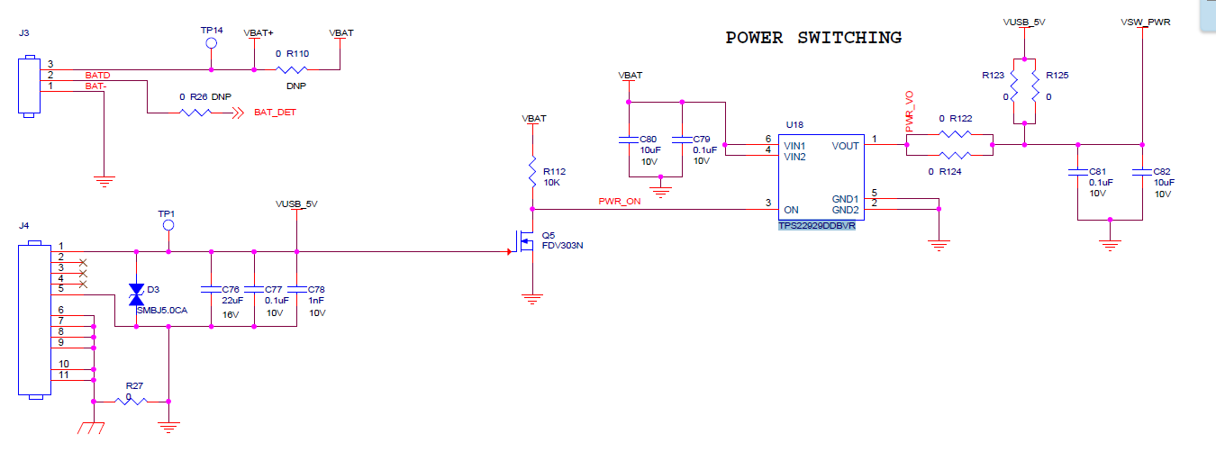
We are using TPS22929D as a power switch.
Attached is the snapshot of the schematic for the power switching section.
This is the functionality:
1) When VBAT is available and there is no VUSB_5V, then the ON control for TPS22929 is high and VOUT= VBAT
2) If both VUSB_5V and VBAT are available. Q5 NMOS would turn on, thereby disabling the TPS22929 and VOUT is disconnected from VIN.
- In this case VUSB_5V is directly connected to the output of TPS22929
- I have few questions regarding this: I read from datasheet that when TPS22929 is off, a 150 ohm load resistor will be enabled to bring down the o/p to 10% value. Since In this case, it will not be able to discharge the o/p ever, will it have any implication on the operation of this IC? Any damage on long term usage in this operation?
3) In case VBAT is not available and VUSB_5V is available. VUSB_5V will be connected to the O/P while the switch is off. Do you expect any issues/anomalies in this case while VIN is 0 V but VOUT is 5 V?
Thanks,
BR,
Ashutosh
