This thread has been locked.

If you have a related question, please click the "Ask a related question" button in the top right corner. The newly created question will be automatically linked to this question.

LM46000 Low output

Other Parts Discussed in Thread: LM46000

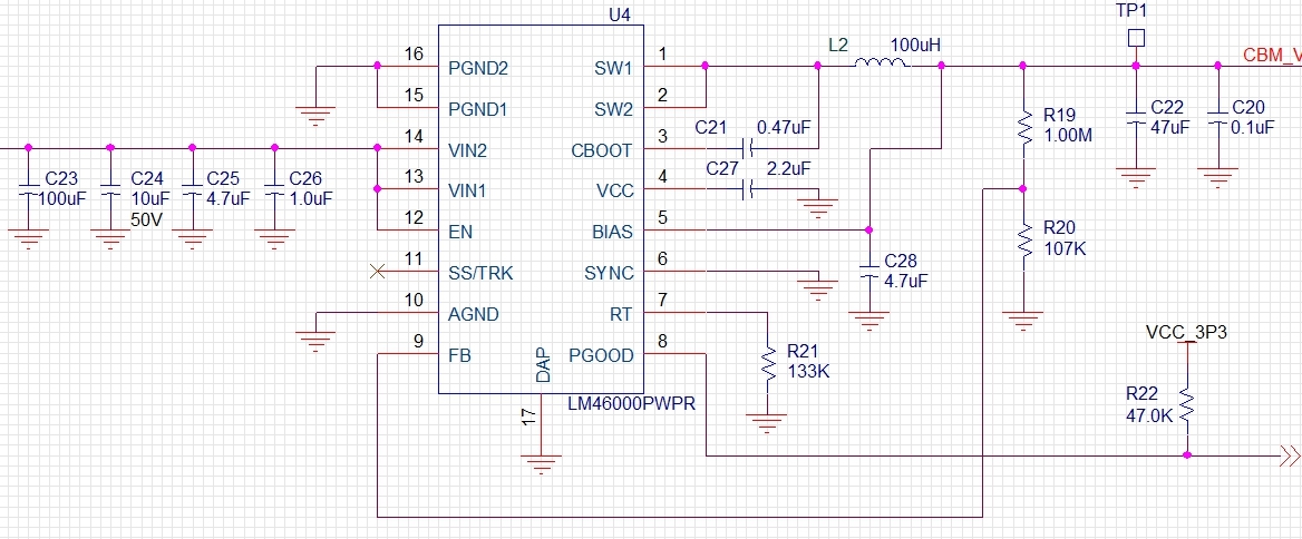
I'm trying to use the LM46000 to generate ~11V from a nominal 14.4V supply.

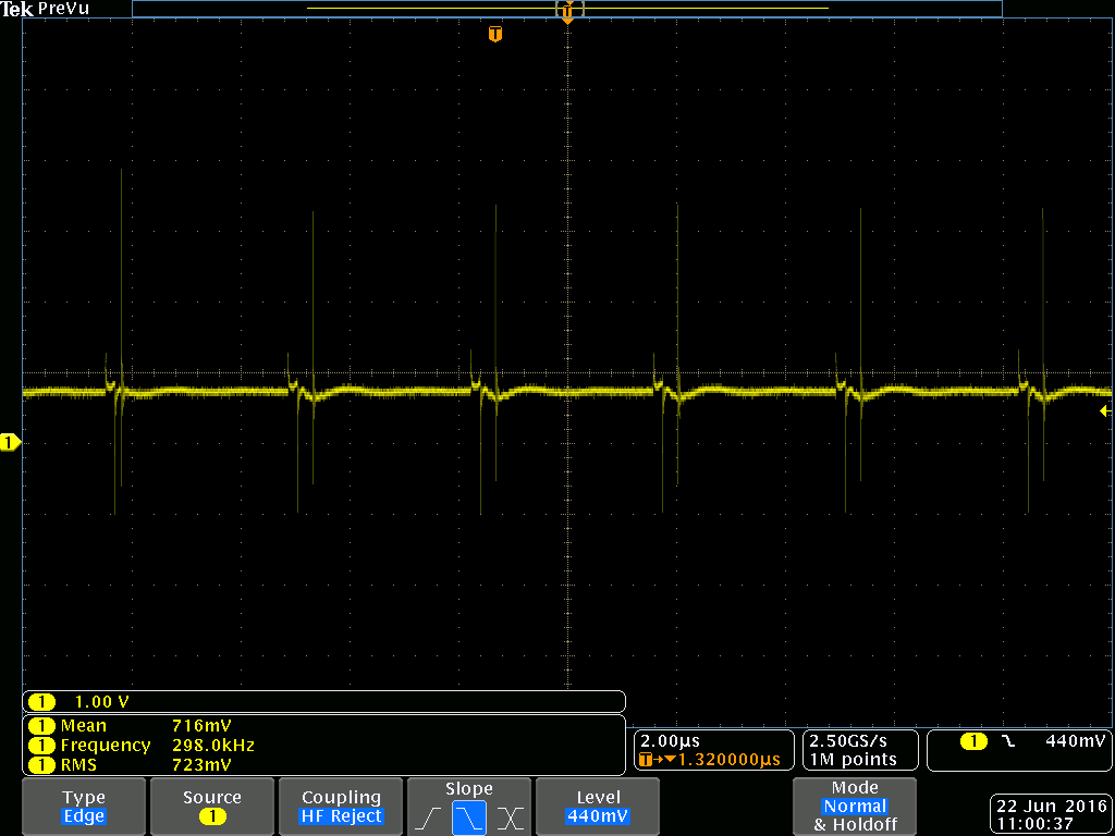
The has some switching action happening, but the switch pin doesn't 'appear to swing to Vin or Gnd like I would expect.

The output only goes to ~0.6V.  When power is 1st applied, the output goes to approximately 0.58V, then climbs over a period of approximately 10 seconds to ~0.65V.

Input current is ~ 130-140mA, LM46000 gets warm (eventually too warm to hold your finger on the top, even with the 'thermal vias' under the DAP).

The FB pin appears to have the 'correct' ratio of Vout present (~1/11th).  I've tried lowering the Rfbt and Rfbb each by a factor of 10 from those shown below with no effect.  Input current remains the same over an input range of ~ 8V - 20V (at 8V, it drops to approximately 0).

There is no load on the part - the load is a module not yet installed on the PCB.  I haven't yet tried a capacitor in parallel with the 'upper' feedback resistor - can't see how that would solve this particular problem.

  • Hello,
    If you are not getting any output and your IC is heating up there could be an issue with the board or connections. Please make sure you dont have any shorts from VIN to VOUT, VIN to ground, VOUT to ground, SW to ground, etc. Please also send us your layout for debugging.

    Regards,
    Akshay
  • Attached are gerber files for the PCB.

    Note that the trace between pin #2 and Pin #5 on the PCB under the part was cut and a jumper added to connect pin #5 to Vout (mistake on original schematic)


    Vin has 14.4V, measured.

    Vcc of LM46000 is ~3.3V, Measured.

    CBOOT has ~3V, measured.

    Part is 'running' - there is evidence of switching (although not a correct looking waveform) on the SW pin(s) - see attached scope shot.  The frequency appears correct for the value used on RT (133K) ~= 300kHz

    Waveform @ SW pins:

    Gerber files:

    520-08027 FOR TI REVIEW.zip

  • Chris,
    I saw the message now. Let me review and I will get back to you. I forgot to mention that it'd be easier if you could send pictures of the layout instead of gerbers. If you still can, it'll help.

    Regards,
    Akshay
  • Could you print above gerber file, or layout file to pdf for us to review please?

    Looking at your schematic, I think the inductance value is too high. This is a high duty cycle operation, 100uH only give about 75mA peak to peak ripple current. Please try a 47uH instead.

    To debug your board, please follow this procedure:

    Check VIN pin voltage presence, check power supply current limit is not too low.

    Check EN pin voltage, should be the same as VIN in your design.

    Check Vcc voltage, should be around 3.1V (VCC presence means part is enabled correctly)

    Carefully probe FB pin voltage, should be around 1V if part is in regulation.

    If FB voltage is 1V, but you still have no output voltage, check resistor connected between Vout and FB

    If FB voltage is not 1V, check SW node waveform by an oscillascope. The SW node should have very wide duty cycle trying to bring up FB votlage. SW node high level should be around Vin

    If all these test still cannot bring up the board, please send us these waveforms:

    VIN, EN, SW, VOUT

    Thank you,

    Yang

  • Picture of layout attached.  Note that the internal trace from Vout to Fb divider was bypassed with a wire on opposite side of ground plane to eliminate potential interference from SW pin - no change in behaviour.

    LM46000_LAYOUT.rtf

  • Hello,

    Here are the observations:

    1) The top layer has no heatsinking for the IC and the SW node. This explains why your device heats up.
    2) The connections to VIN, SW and ground should be copper floods and not just traces. Having copper floods reduces board parasitics greatly. Having trace connects for the power path adds these inductances and causes spikes and unstable behavior
    3) Your output feedback to the upper feedback resistor is directly under the inductor. This will couple noise on it. If you want to route that trace on an intermediate layer, you should plan to have an unbroken ground layer in between as a shield.
    4) The lower feedback resistor ground is very far from the AGND pin of the IC. They should be physically very close.
    5) Capacitors C24,25, and 26 should be connected between VIN and PGND and should be places very close to the IC.

    Your layout does need to improve. The problems you are facing can be directly caused by that. I would encourage you to look at the example layout in the datasheet for more information.

    Regards,
    Akshay

  • Hi Yang,

    I have ordered 47uH and 68uH inductor samples to try.

    Is it typical for this part with too large inductance to cause Vout to remain below 1V?

    I wouldn't expect this kind of behaviour due to excessive inductance, but don't have any prior experience with this part.

    If you read my prior post, you will see that I've measured the items you mentioned.
    SW and Vout are essentially the same voltage, but at SW pin, there is evidence of switching (see picture), while at Vout, this isn't apparent because of output capacitance. Vcc has reasonable voltage, as noted above.

    Should have the eval board this afternoon... I can try our 100uH inductor on the eval board to see if that is the issue.

    Chris