


Hi all,
I'm designing a boost DCDC with a variable output, where efficiency (and BOM cost, and size ... ) is a concern.
Vinmin = 3V
Vinmax = 4V
Vout = 5-20V
Pout = 20W
I think the LM3478 is the most well suited IC for the application, but I'm struggling at different areas. At first, I guessed 350 kHz would be a good compromise. Here's the proposed schematic.

From the proposed WeBench solution, I noticed the transistor was the part that was toasting the most, reaching 75C.
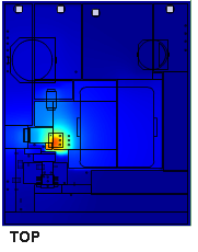
From my limited knowledge, steady state simulation indicates that most of the transistor losses occur at switching.

What can I do to reduce them? Here's a list of option I've been considering:
1) Change the switch. My understanding is that I need a switch with a lower Vth and a smaller gate charge. I haven't found one. :-( It seems the Rds on is not a big deal. Am I wrong?
2) Use an external gate driver, maybe with a bigger MOS or with another MOS in parallel.
3) Reduce the frequency and increase the inductance.
Are there other options? Can someone advice?
Also, I haven't successfully added parallelised components to the WeBench shematic editor. Where can I find instructions? More specifically, I tried to parallelise the Schottky diode and haven't found the Toshiba CMS06 (as proposed initially) in the proposed list.
Thanks in advance!
P.S. I truly enjoy TI design tools and community. Cheers!

