This thread has been locked.

If you have a related question, please click the "Ask a related question" button in the top right corner. The newly created question will be automatically linked to this question.

BQ76200 output fail

Other Parts Discussed in Thread: BQ76200, BQ78PL116, CSD19536KCS

Hello,

I have a lifepo4 16S BMS with a BQ76200 driven by a BQ78PL116.

Sometime the BQ76200 fails : on the chg and dsg outputs, I can observe shorts pulses at 80kHz ... It seem that charge pump is not ok.

Charge pump = 9.25V
CHG_EN, CP_EN, DSG_EN = 2.5V
Vbat = 53V

The only way for fix this problem is to change the BQ76200.

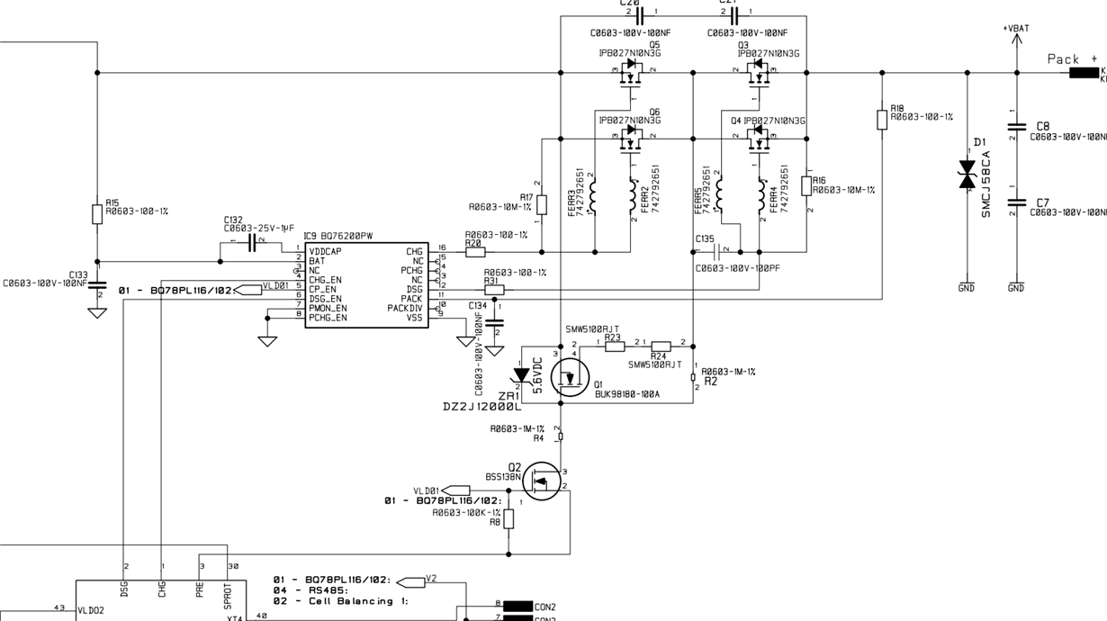
My schematic :

Why the IC fails ?

Thanks

Nicolas

  • It is hard to determine why an IC fails from just the schematic, test and analysis of the part may be needed.

    A first question may be if the IC is really damaged or if it has just encountered a different operating condition from previous operation. The 9.25V seems to indicate the charge pump is operating at about its UVLO level. The pulsing on CHG and or DSG indicates the driver is not able to turn on and is pulling the VDDCP down to the UVLO level. Possibilities are damage to the driver or too much loss during switching. Losses increase with voltage.

    The datasheet recommends a 10 nF filter capacitor for PACK in table 2. Your schematic shows C134 as 100nF. When turning on DSG at higher voltages the part will limit the voltage between DSG and PACK terminals dissipating the CVDDCP voltage into the filter cap (C134) and internal losses before the FET can come on. You might try to apply a charger to pre-charge PACK+ and PACK (C134) before switching to see if this could be the issue. Also I dont' recall how the bq78PL116 sequences the CHG and DSG outputs. It is more difficult for the bq76200 to switch both CHG and DSG simultaneously. I believe the bq78PL116 has FET disable inputs to allow you to control the outputs, you may try to turn on CHG or DSG to determine if the bq76200 can switch its outputs individually or isolate which driver is damaged. If the issue is the voltage reducing the C134 value might help.


    If the IC is damaged, it is likley due to excessive voltage or current. The FET gate capacitance can both raise the voltage of CHG and DSG and push current into the pins through R20 or R31. Smaller filter cap values will allow BAT and PACK to rise faster with CHG and DSG to reduce current into the pins. Larger values for R20 and R31 will also reduce current into the pins but also affect switching speed. Remember that the maximum voltage on the IC is 100V. If BATT+ and PACK+ are going to 100V, CHG and DSG will be ~ 12V above and exceed their abs max even if the BAT and PACK pins are filtered.
  • Thank you for your reply.

    I made a new test with a 10nF filter for PACK and BATT+.
    After some cycles, the BQ76200 fails. The chip is really damaged (there is smoke).

    The BQ76200 fails when the BQ78PL116 drives the DSG output, and CHG = 1.

    Do you have an idea ?

  • If the IC is smoking, one or pins must have have a low impedance to ground.  The likely causes are high voltage onto the pins or high current into the pins.  You will likely have to test to see what is causing the problem.  Typical system transients are from:

    • Switching of the load by the powered product causing high voltage transients
    • Switching of the discharge protection FET fast enough to provide a high voltage transient on the battery (UV with load, OC or SC, high voltage on BATT+, CHG)
    • Loss of load of the charger causing a high voltage spike when the battery protects (OV, high voltage on PACK+, DSG)
    • Fast rise of PACK+ from charger application (plug in or turn on, high voltage on DSG)
    • Uncommon, reverse polarity on the pack. (high current from IC DSG, PACK, current into BAT)

    Your schematic has the filters on BAT and PACK pins.  D1 would be  conducting if there were a high voltage on the PACK+.  CHG and DSG gate resistors R20 and R31 are shown as 100 ohm, these seem a little small.  If you have a 50V battery which switches DSG off quickly there may be a large transient on BATT+.  CHG would be ~12V higher, and although it is trying to follow the filtered BAT pin, the FET gate capacitance will pull on it.   Larger R31 would switch DSG more slowly reducing the Ldi/dt transient, larger R20 would reduce current into CHG. However this is just a possibility, you must determine what is causing the problem in your system.

  • The problem is the Cgd capacitance.

    One of your documents says :

    When using a minimal number of FETs (1–2) under increased battery pack voltages, that is, 48 V, and a
    short circuit occurs, the CSD19536KCS FETs Cgd capacitance requires an increase of approximately 220
    pF in order to provide feedback to keep the gate on as it switches.

    ...
    Refer to your FET manufacturer’s data sheet to determine ideal use.

    So I added 470pF and it works :)

    Now, I have 3 FETs SUM70040E. Cgd = 165pF and Cgs = 5100pF.

    How to calculate the capacity that needs to be added? I tried 470pF but it not work.

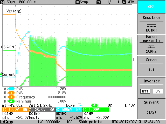
    The FETs fail again when short circuit occurs, with the same problem :

    Nicolas

  • Hi Nicolas,

    I believe you are referring to page 7 of the FET Configurations for the bq76200 High-Side N-Channel FET Driver application note.  As the app note indicates consult with the FET manufacturer to help determine if Cgd is an appropriate solution to your issue.  I think the Cgd value may be an empirical selection dependent in part on the layout.

    DSG from bq78PL116 is a 2.5V signal.  In your waveform the DSG_EN starts at 2.5V but appears to go below 0V, then comes up and oscillates above the high voltage.  I have not used the bq76200 with bq78PL116, but when I have observed similar large amplitude signals on DSG_EN it was due to incorrect grounding of VSS on the bq76200.  VSS should connect to VSS of the bq78PL116, DSG_EN should not be able to go below VSS.  There may be some high impedance in the connection or improper connection on the ground which allows the negative voltages and oscillation. Notice that tPROP_DSG is 0.5 us, so response by the part can be very fast.  A cap from DSG_EN to VSS may slow response to let you see what is happening, but you generally don't want to increase the time DSG_EN is in the threshold region by slowing the edge significantly.