This thread has been locked.

If you have a related question, please click the "Ask a related question" button in the top right corner. The newly created question will be automatically linked to this question.

HELP (cooking tps61088‏ instantly) :'(

Other Parts Discussed in Thread: TPS61088, PMP9778

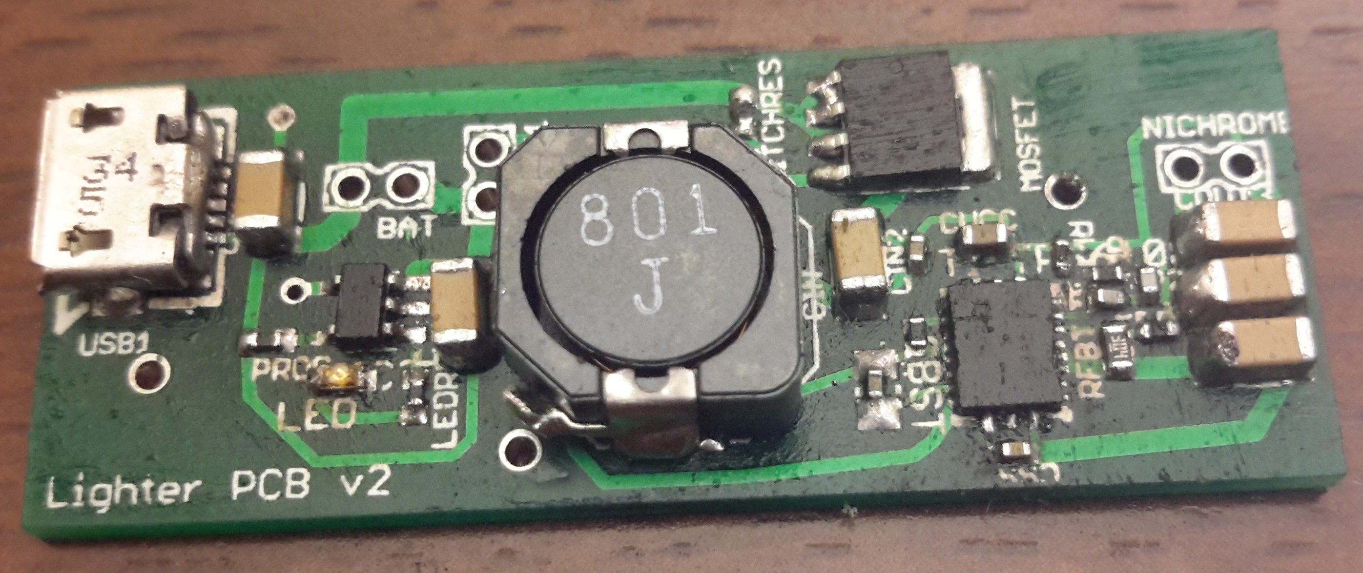
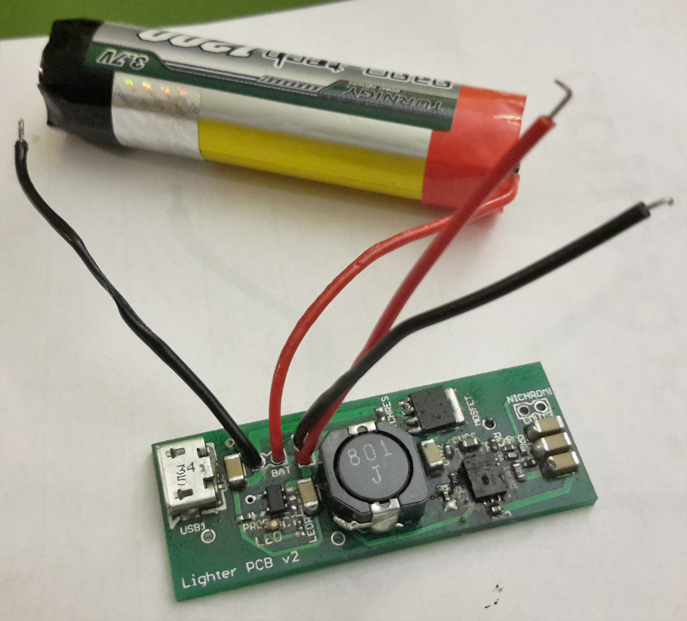
first time i think i did a bad job soldering because i had poor equipment and its vqfn

second time i shorted the battery power to ground accidentally while soldering, maybe that damaged it? but would that cause it to over cook again?

i have not connected a load to the circuit, also the second instance the switch which connects the battery via a mosfet was not on

  • Can you post your schematic? Your pcb layout looks rather marginal.
  • I don'y directly support TPS61088, but it looks like you have some schematic errors with regard to ground connection. I suggest you look at the datasheet to see how AGND and PGND are connected. You should look at the EVM users guide for layout. With that layout, I anm not surprised you are having issues.
  • i did the schematic and pcb and the board so i dont see errors otherwise i wouldnt have done it the way it is and i wouldnt have come here
    i emailed ti so hopefully i will get some support
    the datasheet states clearly that pgnd connects to mosfet source instead of the normal connection to drain
  • The output GND return and SS GND return are only connected to the NC pins in your layout, then back to thru FET (which I assume is you on/off switch) then back thru the long bottom side trace. They should be connected to PGND at the IC directlyThe AGND appears to only be connected to the AGND pin, then connected along with the power return. It needs to be connected to PGND directly as well. The bottom side just has a wide trace. It should be a GND plane. You have thin traces for SW, Vin and Vout. They should be large copper fill areas. There are probably other issues as well. When PCBs are designed this way, there are almost always problems. Let me see if I can find a direct support person for TPS61088. I can't really spend too much time on other product line issues, but that should give you a start.
  • Hi ,


    I'm the application who support TPS61088.


    first, the schematic is wrong. Pin 11, 12, 21, 20 should be connected together. PGND is the boost converter's power return ground.


    Second, the PCB layout is really bad, please refer to  the TPS61088 userr guide and datasheet to get the layout example. Also you can refer to the TI reference design PMP9778 to get more knowledge about the good layout.

    Could you please share the detailed application information for us? Like in what kind of equipment? Volume?  You can send the information to me by email, my email address is helen-chen@ti.com

  • thank you, i think you're right although that means this error is TIs fault and therefore I am really annoyed because I only had 2 components and they are both destroyed now so I have the hassle of getting more now as well as probably getting a new pcb designed.

    first of all here is what the datasheet says which is what I did

    second the circuit was designed by TI inside of TIs online system design software which made the schematic and component selection for me

    I simply exported this to Eagle CAD so that error is not my fault and even though I review the design you can see the datasheet is telling me the wrong thing so basically TI wasted my money and my time.

    I prefer the way LT works with me to design the circuit, initially i thought this was better but i was naive to believe its reliability

  • please take a look at my reply to JT

    to answer your questions:
    it's going to be a hand held device
    the circuit will heat a nichrome wire
    final design will be mass produced
    i dont know quantity, i am freelance

    thank you
  • Thanks for the update.

    Sorry for making you confused.

    Before you begin the design, you should firstly check the typical schematic connection on the datasheet, like the below schematic on page 1.

    then check the layout example on page 20. AGND and PGND should be single point connected.

  • I use the pin explanations to draw a circuit instead,
    as for those 2 diagrams. it's not possible to connect to ground.
    thats actually the reason the circuit is cooking because that is a short directly from VBAT to ground.
    so the only way is for me to connect the PGND to the same as the AGND which is the MOSFET source.
    will that be ok?
    in that case i should change the layout so that the mosfet source is close to the AGND/PGND
    and connect the AGND PGND nets
    and remove the NC nets
    and increase the vias for ground
    and have a ground plane bottom layer
    and a copper pour for SW

    thanks
  • also can i get sent a few more of these chips please, i need to get this prototype working quickly
  • hello, i didnt get an answer to the last couple of questions

  • The NC pin can be connected with PGND and AGND to make the total GND copper plane biger, which is good for thermal performance.


    The FB netwotk, compensation netwotk should be connected to AGND to ensure the stability. AGND and PGND can sigle point connected.
    In a word, you can refer to the PCB layout in the datasheet