This thread has been locked.

If you have a related question, please click the "Ask a related question" button in the top right corner. The newly created question will be automatically linked to this question.

LM2940CS-5.0: Output at 3.1V

Other Parts Discussed in Thread: LM2941

Failure symptom(s)

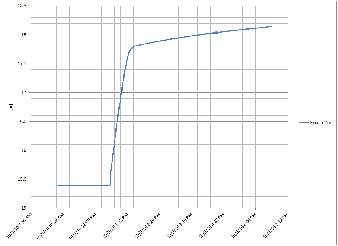
    • After several hours of normal use, regulator output drops to 3.1V
    • This causes 4.096V reference IC to drop, which impacts ADC readings
    • An example ADC reading is shown below

    • Sometimes regulator recovers after a few hours (after setting PCB ground back to 0V)
    • Sometimes regulator never recovers and the output is permanently at 3.1V (even when PCB ground is 0V)
    • In this second case, replacing the regulator brings back full functionality at PCB ground = 0V
  • Would like to know what can cause the output to drop to 3.1V
  • We have a few theories, but we don’t know how plausible they are
    • Unit goes into thermal shutdown as a result of 30 kV and/or 30kV-to-chassis leakage path
    • Unit enters current limit mode due to the 30kV-to-chassis leakage path

Details:

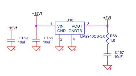
  • Using LM2940CS-5.0 in design
  • Supplying power to several op-amps and a 4.096V reference IC
  • Max load current is ~200 mA
  • Input voltage = 15V (nom)
  • Below is regulator circuit

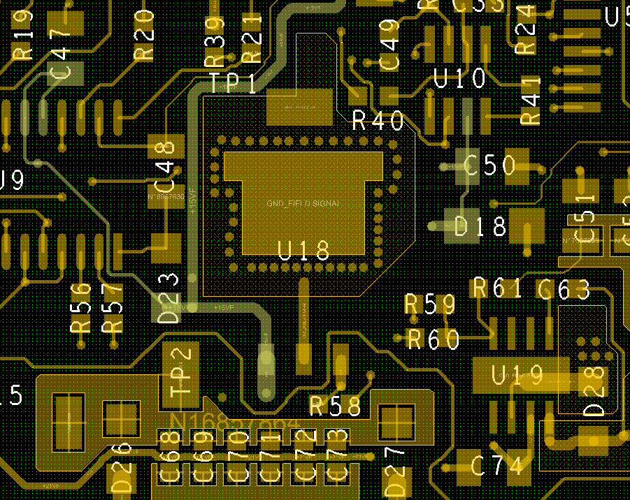
  • Below is regulator layout

Top

Bottom


  • PCB is inside metal box
  • Metal box is filled with potting material
  • Metal box is connected to chassis ground
  • PCB ground is at 30 kV, relative to chassis ground (hence the potting)
    • This is a programmable value

  • Hello Jim,

    From the schematic I see that the output capacitor (C157 10uF) value is low. This should be 22uF minimum.

    It looks like you are using a series R (R58 1.0 ohm) to simulate the required ESR for Cout. The 1.0 ohm value is OK

    For LM2940/LM2941 using ceramic for Cout, I generally recommend going up to 33uF (or higher) for ceramic Cout, just to make sure that 'Capacitance vs Applied DC Voltage' de-rating does not take the final operating capacitance value below 22uF.

    The input capacitor value (C158 10uF) should be adequate, presuming that the input voltage is relatively ~clean~ of voltage spikes, even if the 'Capacitance vs Applied DC Voltage' de-rating with 15Vdc applied is >60%.

    I see R58 on the PCB, but I do not see C157 or C158. The output capacitor (and series R) must be connected as close to the device as possible, directly between the OUT pin and the GND pin, on the same side of the PCB that the LM2940 is mounted.

    As you described, the LM2940CS-5.0 (TO-263) would be dissipating 200mW. In a typical application (this is not typical) this would cause junction temperature rise to be less than 10C above the ambient temperature. In your case, the potting material may have some detrimental thermal issues, but if there is total contact with the PCB surface area and the LM2940 package, my guess is that it would not be significant issue.

    As for "... PCB ground is at 30 kV, relative to chassis ground ...", in ~theory~ it should not be a problem. In practice, this concerns me as the isolation has to be absolute.

  • Hi Donald,

    Thanks for the response.  See my comments below.

    >> From the schematic I see that the output capacitor (C157 10uF) value is low. This should be 22uF minimum.

    There are additional capacitors on the +5Vf net that were not shown in my original post.  The total capacitance is 71.2 uF (7 x 10uF caps + 12 x 100 nF caps).

    >>I see R58 on the PCB, but I do not see C157 or C158. The output capacitor (and series R) must be connected as close to the device as possible, directly between the OUT pin and the GND pin, on the same side of the PCB that the LM2940 is mounted.

    These components are on the bottom layer (see attachment in original post).  What is the downside to placing C157 on the bottom?

    >> As you described, the LM2940CS-5.0 (TO-263) would be dissipating 200mW. In a typical application (this is not typical) this would cause junction temperature rise to be less than 10C above the ambient temperature. In your case, the potting material may have some detrimental thermal issues, but if there is total contact with the PCB surface area and the LM2940 package, my guess is that it would not be significant issue.

    The maximum load current is 200 mA, so the maximum power dissipation is 2W: (15 – 5) * 0.2.  Per the LM2940 data sheet, if the dissipated power is 2W then the delta T is ~80C.

    What kind of thermal issues can be caused by the potting material?

    Regards,

    Jim

  • My apologies for my poor math.

    Yes, 10V x 0.2A = 2W.

    In a normal situation, with normal open air PCB, the thermal resistance from junction to ambient would be 40.9°C/W.

    With two Watts of dissipation the junction temperature would be expected to rise (2W x 40.9°C/W) = 81.8°C above the external ambient. temperature.

    Potting compounds are outside what we can model thermally and certainly are outside the JEDEC conditions for the given RθJA value. Potting compounds can act as an insulator, allowing no air-flow to remove heat, from the LM2940 package or the PCB, or if can act as a thermal conductor to move heat away from the device and PCB to some external heat sink. In these cases it falls on the end user to verify that the junction temperature is not exceeded.

    This may indeed be a case where heat builds up and eventually thermal shut-down kicks in.

    As for the mounting components on the opposite side, the typical problem is that the via introduces an inductance in series with the capacitance, It's not a lot of inductance, but it might be enough affect compensation. It's not always a big deal, but our general rule is : 'don't do it',