This thread has been locked.

If you have a related question, please click the "Ask a related question" button in the top right corner. The newly created question will be automatically linked to this question.

UCC27714: Floating Drive oscillation at Pin 11 of UCC27714

Part Number: UCC27714
Other Parts Discussed in Thread: UC2824,

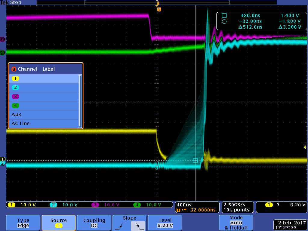
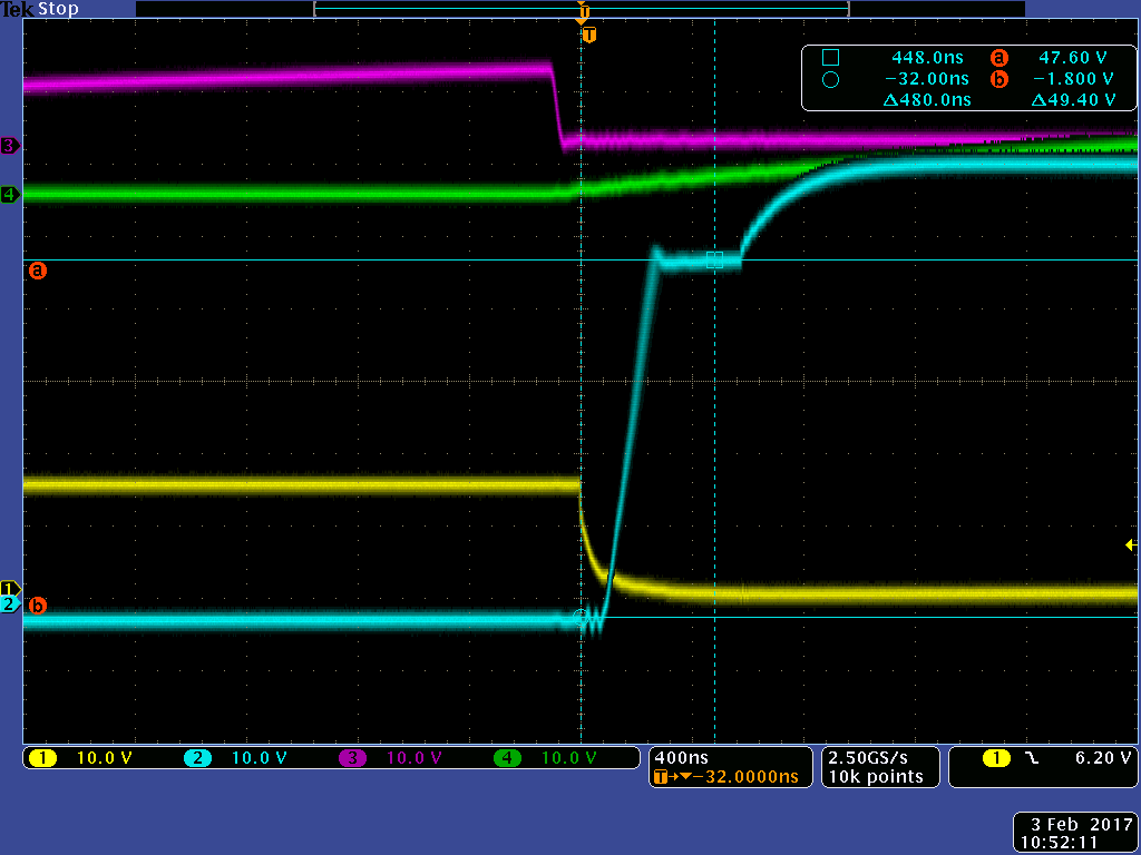
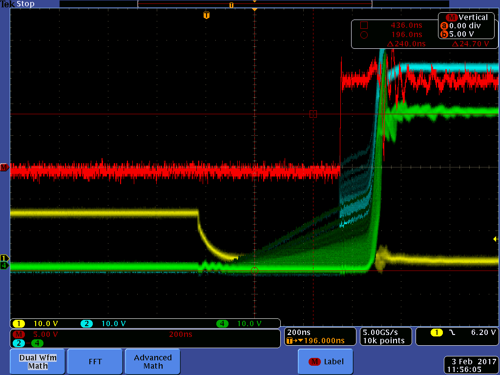
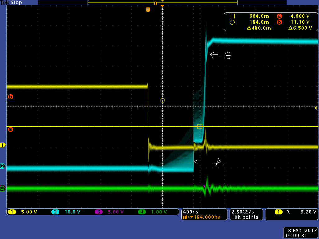
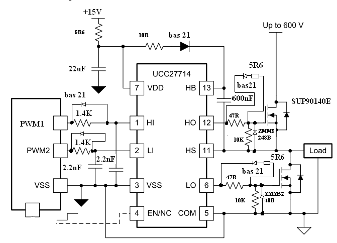
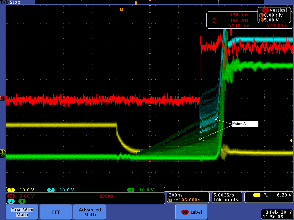
I am using UC2824 to drive UCC27714 and then to N MOSFET SUP90140E.  The waveform is taken on pins of UCC27714 with respect to pin 5. Channel 1 Pin 6 Channel 2 pin 12  channel 3 pin 2 and channel 4 pin 1 . My question I saw oscillation in rise time waveform of channel 2 which is the high side drive for the mosfet. Any idea how to troubleshoot?  Is the oscillation cause by the DC TO DC Inductor ? My design is a buck converter with input at voltage of 45V and output  suppose to be at 28V, I currently unable to  raise the output voltage to 28V  . There is a output load 4 ohm attach to the output capacitor .  Thanks a millions.

  • Hi Lim,

    I have asked one of our applications engineers to contact you. In the meantime you may want to take a differential measurement of the gate drive signal on the high side mosfet by using two channels on the oscilloscope and the subtraction maths function to see the actual gate drive voltage waveform.

    Regards

    Peter
  • Hello Lim,

    As Peter mentioned in his reply, it is important to look at the high side gate drive voltage from pin 12 (HO) relative to pin 11 (HS). If high voltage differential probes are available, the best method is to use a differential probe from pin 12 to pin 11. If differential probes are not available, one probe from pin 12 to pin 5, another probe from pin 11 to pin 5 and use math to subtract 12 to 5 from 11 to 5.

    The ringing on the HO output you show is likely present also on pin 11, the HS switch node. The parasitic inductance and parasitic capacitance on the power train switch node is the cause of the ringing that occurs during the fast rising dV/dt on the HS switch node.

    To reduce the ringing, the recommendation would be to increase the gate resistance value on the high side MOSFET.

  • Hi Richard

    Thanks for the advice. Yes you are correct the ringing is also in Pin 11 with respect to pin 5. I also have an observation, when I did not attached the 4 ohm to the output load, I did not see the ringing. Below is the waveform at the probed at the same location  as of the first graph but without load at output . It seems the ringing only come with increasing load given to the output. Is this the normal observation. Thanks. Will try to increase the gate resistance to see if the  ringing situation improve. Thanks

  •  Hi Richard

    After changing the gate resistor from 47ohm to 94ohm. The ringing issue upon loading has not improved, should i try to increase the gate resistor value some more ? Attached is the capture waveform.ch1 -pin 6 ch2- pin 12 ch 4 pin 11. The ringing appear simultaneous both on pin 12 and pin 11.Thanks a millions

  • Hi Peter & Richard,

    Another symptoms noted is that, if the setup is hooked up with a 8 ohm as load, as I tuned the output voltage from 0V  to 28V, during the initial voltage rising,  the ringing goes up to a certain threshold and then ringing disappear on the way to 28V. There is no "short through" causing mosfet failure. Whereas  in the 4 Ohm case, as I tuned to  the output voltage up to 28V, the ringing is do bad that it cause a "short" through, any advice on going forward ? Thanks a millions

    Regards

    Hoon Sin

  • Hello Hoon,

    The behavior you describe regarding the load conditions increasing from 8 Ohms to 4 Ohms is likely caused by the power stage being in a soft switching condition at lighter load, and hard switching at the higher load. When the inductor current is increased to the point that the valley of the ripple is positive (over zero), during the dead time between the low side FET conduction and high side FET conduction the body diode of the low side FET will conduct the inductor current. When you turn on the high side FET, the low side FET body diode is forced off (after the recovery time. This results in much higher VDS dV/dt and ringing will increase.

    The ringing on the high side gate drive may be high enough to force the driver output below ground by more than the device rating. To resolve this, place schottky diodes from the driver output to clamp to HB and HS. One diode anode is connect to HO and cathode to HB, the other diode cathode is connected to HO and anode to HS. Place the diodes as close as possible to the IC pins. See below for the diode placement.

    For the experiment place clamp diodes for the LO output as well.

  • Hi Richard.

    Thanks for the reply. I have implemented the back to back  schottky diodes as in pin 13 pin 12 and pin 11 of UCC27714. Below is the waveform captured at ch1- pin6 , ch2 -pin 12. The ringing at B has improved but not the ringing at A. Any thought on this observation ? Will try the the same mode on pin 6, pin 5 and pin 7. thanks


  • Hi Richard. Have try the same back to back  implementation on pin 5 pin 6 and pin 7. The Ringing on point A did not improve. Any idea what is cause of ringing on point A . Thanks 

  • Hi Richard

    The Ringing seen at point A   is it detrimental to the operation of the switching? I have observed that if I change to load to 4 ohm, this Ringing becoming worst so much so that it reduces the dead time between H0(pin12) and L0(pin6) causing failure to the Mosfet (as i increase gradually the output voltage to the desired 28V). Thanks


  • Hi Richard/Peter/John

    No sure if you have any advice for me on the way forward. Thanks for the help so far.

    Regards

  • Hi Richard/Peter/John

    In the Datasheet UCC27714 page 26, it specified that if HS were to be negative to COM , H0 might be force to +ve with respect to HS even if Hi is shorted to ground. Upon the LO switch off   the lower Mosfet in any DC to DC Converter  there is a chance that body diode in Lower Mosfet is conducting thereby causing the HS to be negative with respect to COM. Would it explain those Ringing at point A in my waveform ? If this is case, do you have any solution for it. thanks

    Regards

  • Hi Lin,


    Richard is our best technical resource to support your application but he is based in the US and it will be a couple of hours before he is on-line.

    Regards


    Peter

  • Hello Lim,

    Page 26 in the datasheet does show the negative voltage ability of the UCC27714 on the HS pin. The driver IC has been tested at various negative voltage levels and time duration, to determine if the outputs stay in the correct state. The negative HS voltage when the output can be in the incorrect state is beyond -15V by the Figure 53 graph for a very long duration. The datasheet recommended operating conditions show a -8V DC capability on the HS pin relative to COM.

    The scope plots you show indicate a negative voltage as expected with body diode conduction, but the level is -1.5 to -2V by estimation. This level on the HS pin is expected and should not create incorrect output states.

  • Hi Richard

    Is the phenomenon(ringing) at point A normal observation for UCC27714? If not, what can we do to reduce these ringing at point A. Thanks a millions

    Regards

  • Is the phenomenon(ringing) at point A normal observation for UCC27714? If not, what can we do to reduce these ringing at point A. Thanks a millions

    Below is the attached schematic to assist in the understanding of the issue.Thanks

  • Hi Richard/Peter/John
    Not sure if you guys have any good guidance for me to resolve in this issue ? Thanks a millions
    Regards
    Hoon Sin
  • Hello Lim,

    I am not sure what time you refer to as point A. But the ringing on the HS node, and ringing that will appear on HO (relative to COM) is common with half bridge power trains due to the parasitic capacitance and inductance on the power train switch node.

    Are you still having behavior issues, after trying some of the suggestions such as increased gate resistance, and/or clamping diodes on the HO and LO outputs?

    Or is there still a desire to reduce the ringing amplitude, and the power train is working properly?

    One thing I notice, that may be a concern. The signals into the LI and HI pins appear to have a very slow rising time. I assume there is a desire to program delays with the driver input signals, can you confirm? It is always recommended to have fast rising and falling times on the driver inputs to avoid the possibility of the driver false triggering from ringing that may be present on the driver inputs. If the input signals are fast rising and falling, the input thresholds will be largely exceeded during possible ringing. If the rise or fall is slow, the ringing amplitude is much more likely to trigger the driver.


  • HI Richard

    Thanks for your inputs.

    The point A is referring to the rise time Ringing(Or False triggering). It is as shown in the above Diagram. Yellow - LO drive Pin 6 UCC27714. Blue - HO Drive Pin 12 & Green- HS Pin 11 .Red is the Mathematical subtraction of waveform  Blue and wavefrom Green which is  the drive signal seen by the High side MOSFET.

    During the course of investigation, I also collected another waveform this time output not loaded and the ringing is missing. The Red colour waveform which represent the drive signal seen by the high side mosfet look unaffected when comparing between the two diagram. - Does this mean the drive signal Hi Li  are not cause of Ringing at point A ? 

    I have tried back to back diode solution at the high side HO and Low side LO, the Ringing at point A has remained the same.

    Just to confirm  again that,  the Point  A Ringing is  normal and  cause by parasitic Capacitance an inductance at the switch node. I could not find from Web any information regarding this types of Ringing. Most is on the overshoot Ringing that might cause high side Mosfet to fail.

    For this type Ringing at Point A, would you be able to share any literature on it ? Thanks millions


  • Hi Lim,

    You might want to uncheck Question answered few posts back. Are you still having this ringing @A ? if so perhaps the zener protection diodes placed directly on the gate of the MOSFET are causing it. Infineon suggest in parallel MOSFETs to put them in front of the gate drive resistor to stop oscillation. The HO/LO gate drive source resistance 3.75 ohms plus the series impedance of 16v zener might be enough alone without adding a series resistor on the cathode.

    For that reason we opted for 16v zener where 15.25v Min 16.2 max. It is plausible 15v zener starts conducting 13.8v during commutation causing parasitic gate oscillations. Oddly @A seems to occur inside the Miller plateau around 15v (CH2) output and seems to ring even when output (CH2) is unloaded in the same area..