This thread has been locked.

If you have a related question, please click the "Ask a related question" button in the top right corner. The newly created question will be automatically linked to this question.

UC3879: Phase shifted full bridge converter

Part Number: UC3879
Other Parts Discussed in Thread: UCC3895, UCC28950

Dear all,

I am redesigning a full bridge converter as a Phase shifted full bridge converter using UC 3879.

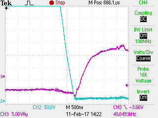
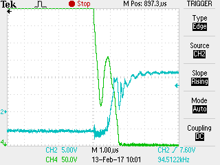
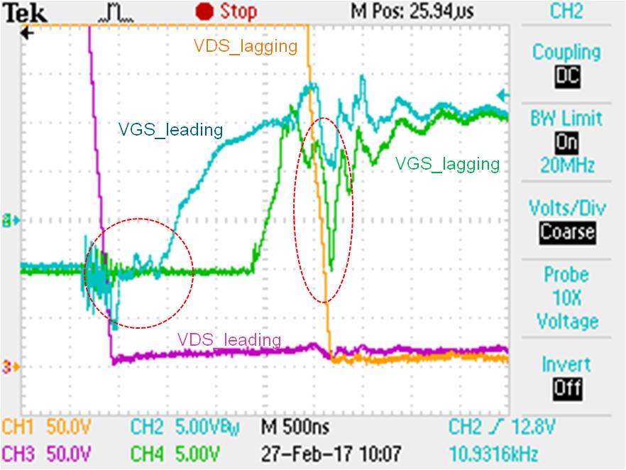
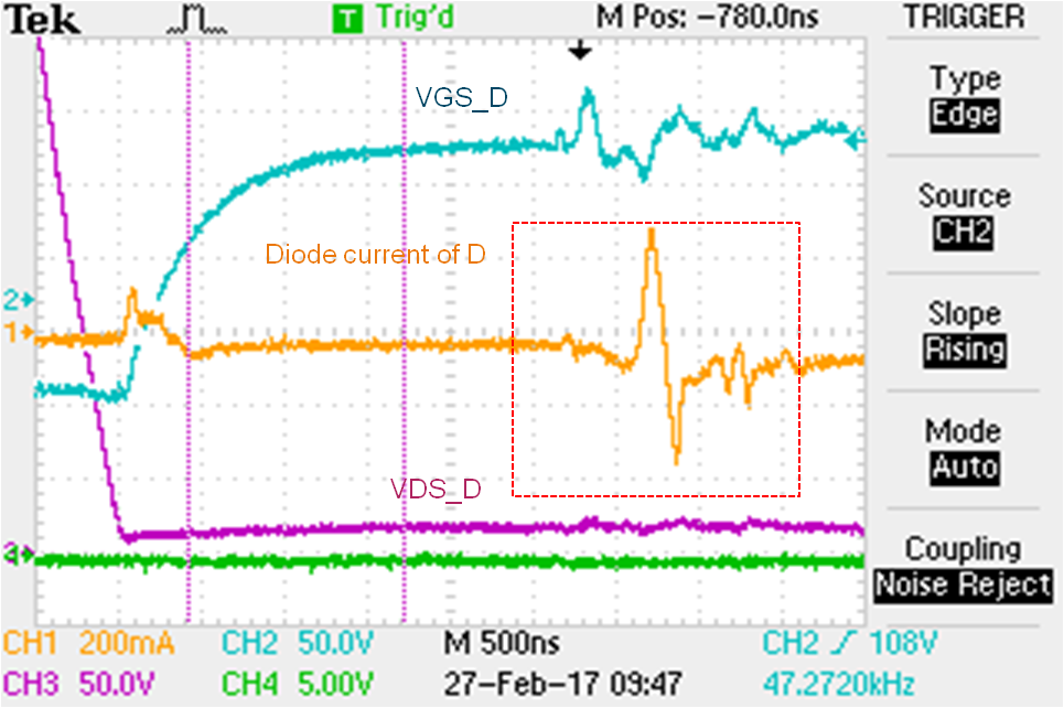
I have a series capacitor in series with primary of the transformer. And a snubber across the MOSFET.\

How this two components affect ZVS behavior , Is it required a series capacitor for this application?

  • Hi,

    For phase shift full bridge, since it is zero voltage switching, you do not need snubber. If you are doing voltage mode control, you will still need the series capacitor to block DC voltage, it will not affect ZVS.

    Regards,
    Bosheng
  • Dear Mr sun

    I am able to achieve ZVS in Leading Leg in small Load current but when current is increasing an oscillatory behavior is starting to take place in VDS
    please find below design details

    Mosfet:IXFN38N100Q2 Coss=950pF

    L_leakage of transformer=11.3uH

    L_magnetising of transformer=17.793mH

    Vout=24V

    Pout=2.5Kw

    Vin_nominal=600VDC

    Removed snubber but response is not changing.
  • Hi, HARIKRISHNAN,

    I am working on that, will get back to you soon.

    Regards,

    Bosheng

  • Hi, HARIKRISHNAN,

    Can you show some VDS waveform? Did you try to tune the control loop?

    Regards,

    Bosheng

  • Dear Bosheng

    Please find waveforms

    1) Low output current ZVS is visible

    2) High output current VDS is oscillating

    Thank you

    HARIKRISHNAN

  • Hi HARIKRISHNAN,

    Please try to reduce the deadtime.

    What is the value of your resonant inductor?

    Regards,

    Bosheng


  • Lresonant=11.2uH

    not added shim inductor , only leakage inductance of transformer used

  • Dear Bosheng,

    I have added a 10uH inductance in series with the primary of the transformer and checked the wave form
    now the inductance is 11.2uH leakage plus 10uH inductance
    even though lagging leg is not going into ZVS please let me know any other corrections to do

    HARIKRISHNAN
  • Hi Harikrishnan,

    I have asked an expert to look at this, he will help soon.

    Regards,
    Bosheng
  • Dear Bosheng,

    After some mathematical calculations I have concluded that energy available for lagging leg to go into ZVS is not sufficient at my current

    please look into the following difficulties I am facing

    The lagging lag is not going into ZVS but the gate voltage is reducing to zero after turning it ON why?

    Can you suggest some thing

    HARIKRISHNAN T

  • Hi HARIKRISHNAN,

    Looks like the glitch was caused by the stray inductor in the source of power MOSFET. The turnon and turnoff current loop paths (PWM output/driver, power MOSFET and bypass capacitor) must be minimized as much as possible in order to keep the stray inductance to a minimum. High di/dt is established in these loops at two instances during turnon and turnoff transients which induces significant voltage transients on the output pin of the driver device and Gate of the power MOSFET.

    Thanks
    Oliver

  • Dear Oliver,

    Thanks for your response

    I did the same experiment (Same mosfet and Power components) with UC3525 ( full bridge controller) and the wave form is smooth without any glitch

    Is there any specific reason for the same in PSFB?

    see the glitch is coming after MOSFET is fully turned On

    HARIKRISHNAN T

  • Hi HARIKRISHNAN,

    I believe this is more related to PCB layout and drive capability of the controller rather than topology of the converter. It seems that the glitch was happened at the Miller Plateau (Vds falls) so the we can't say the MOSFET was fully turned on at that time. 

    Thanks
    Oliver

  • Hello Harikrishnan

    The gate voltage is dropping almost to zero due to miller capacitance effects. In the absence of ZVS the high dv/dt at the MOSFET drain partially discharges the gate / source capacitance of the device. What you are seeing is a severe form of the 'Miller Plateau'. If you achieve ZVS, then the drain voltage is already zero at the time that the MOSFET is turned on and there is no dv/dt to discharge the gate/source capacitance.

    The ZVS transition happens much more quickly when the system is at full load. In your case you should try to reduce the dead time at full load.

    The UCC3895 device and the newer UCC28950 device offer an adaptive delay function so that the delays are modified automatically to take account of the way the optimum dead time varies as a function of load current.

    Regards

    Colin 

  • Hello Mr.Colin

    After reducing the dead time I have experienced cross conduction in leading leg.

    I have added 20uH inductor in series with the transformer and this issue got resolved

    Leading leg is now switching in full ZVS and lagging is in partial ZVS and I got nearly 3% more efficiency than normal full bridge. I have conclude my primary current which is nearly 4A is not enough for lagging leg to go into ZVS

    But 30uH leakage inductance is not an acceptable solution as oscillations in the drain current is too high and my devices are blowing while running in full load for some time.

    Please find below design values

    Input 600 VDC

    output 110V DC

    Power 2.5KW

    transformer magnetizing inductance-17.793mH

    Transformer leakage inductance-11.3uH

    Coss=950PF at 25V

    Transformer ratio=34/9

    Lout=230UH

    Regards

    HARIKRISHNAN NAIR

  • Hello Harikrishnan

    I'm glad to see that you have made some progress -

    There are a couple of things that could be causing the over current oscillations 

    1/ There is a possibility for an over voltage condition to occur as the transformer comes out of freewheeling. This can be clamped by adding some diodes as shown in Figure 48 of the UCC28950 (also a PSFB controller) - copy shown below.

    2/ It may be that there is some un-clamped inductive ringing due to a PCB layout issue

    3/ Your transformer has a very low leakage inductance in proportion to its magnetizing inductance. This is normally a good thing but it also implies that the transformer has a very high inter-winding capacitance. Switching action can drive fairly large currents through this pri/sec capacitance leading to ringing on the current sense signal. 

    Could you post a schematic, a plot of the CS signal and a plot of the drain voltage waveforms. If you wish you can send them directly to me at colingillmor@ti.com -

    Regards

    Colin