This thread has been locked.

If you have a related question, please click the "Ask a related question" button in the top right corner. The newly created question will be automatically linked to this question.

TPS74001DGKR more than expected output voltage

Other Parts Discussed in Thread: TPS740

Hi,

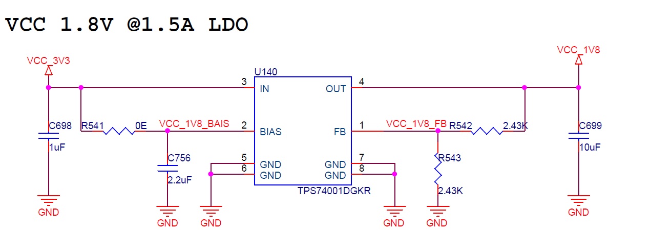
I'm using TPS74001DGKR in my board and I have designed it for 1.8V output.

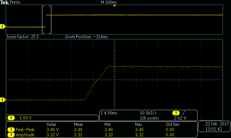
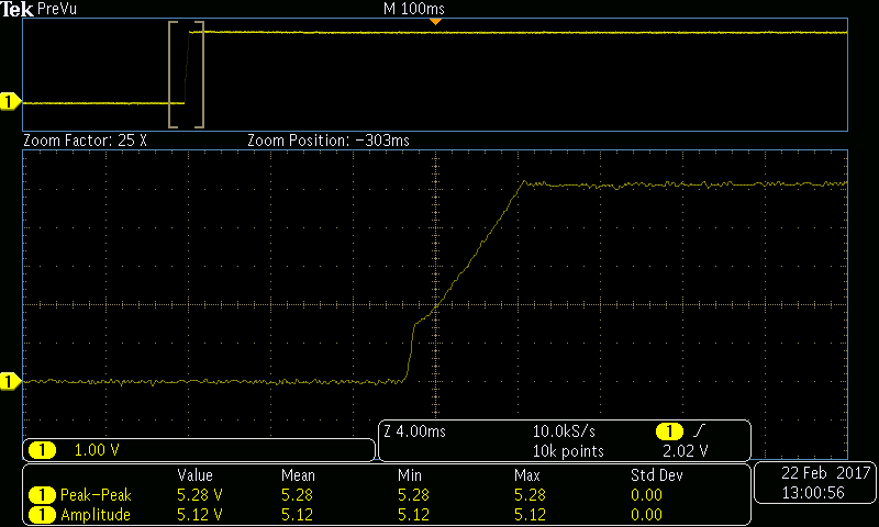
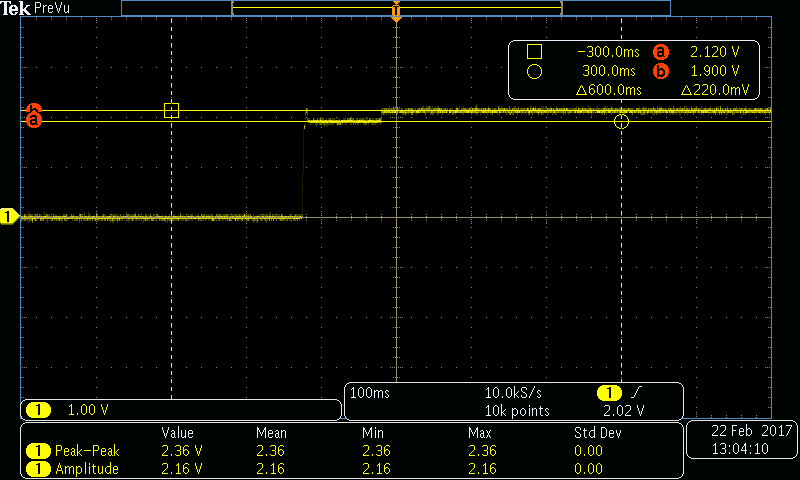
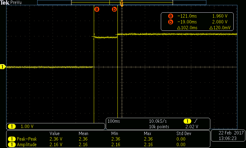
I'm finding that the output voltage is more than specified voltage. (2.02V)

The part circuit schematics is as shown below.

If anyone knows the reason for this behavior of the IC, please let me know ASAP.

Thanks & Regards,

Nanjunda M

  • Hi Nanjunda,

    In order to help debug, could you provide scope shots of Vin, Vout, and if possible Iout? Please make one of them a startup waveform.

    The most likely cause of the TPS740 output being higher than it is set to is an unintentional bias on the output. Could you describe the load for the LDO? Are there multiple voltage rails powering the load? Is there a leakage path caused by left over flux from soldering?

    Very Respectfully,
    Ryan
  • Hi Ryan,

    (Note: Vin = 3.3V, Vout = 1.8V, Iout = 0.5A)

    As indicated in the circuit diagram, input supply voltage is 3.3V (3.20 is the exact voltage we are observing at the input of the IC)

    The maximum current requirement is 0.5A for the board as per the theoretical calculations. The required output voltage is 1.8V.

    The output is connected to few level translators(TXS0108EPWR) and a Wifi Transceiver(ODIN-W160).

    Yes, there are other voltage rails(3.3V) connected to the device and as per observation there is no leakage path on the board.

    Please help us on this issue ASAP.

    Thanks & Regards,

    Nanjunda M

  • Hi Ryan,

    I removed the 0E resistor connected to VCC_3V3 from bias pin(pin 2) and connected 5V through a wire to check whether it is the bias voltage issue, but still I'm observing output voltage of 2.1V.

    Please suggest us, how can we proceed ?


    Thanks & Regards,
    Nanjunda M
  • Hi Nanjunda,

    In order for me to help debug, please provide the requested scope shots of Vin, Vout, and if possible Iout.  One of these scope shots should be a startup waveform.

    If it is possible, disconnect the load from the TPS740.  There may be a leakage path within the load from the 3.3V rail that is also powering the load.

    Very Respectfully,

    Ryan

  • Hi Ryan,

    In my board its not possible to Isolate the supply voltages.

    I have attached the Vin and vout scope images below.

    Vin=3.3V

    Vbias=5V

    Vout =1.8V

    Please help us.

    Thanks & Regards,

    Nanjunda M

  • Hi Nanjunda,

    From your Vout scope shots there is a voltage step 100ms after the LDO starts up. There is nothing within the LDO that would account for this voltage step. The most likely cause of this step is a bias on the output of the LDO. Many times in devices that require multiple voltage rails (such as yours), there is an unintentional path between the power rails. Often this path is through protection diodes. Traditional LDOs do not sink current; therefore, when the output is biased high, it is up to the load itself to pull the output down to the set voltage. If you add a resistor from Vout to GND you may be able to defeat the bias on the output of the LDO, but this may not be necessary in your application since it appears that the bias is coming from the load itself.

    Very Respectfully,
    Ryan