Because of the holidays, TI E2E™ design support forum responses will be delayed from Dec. 25 through Jan. 2. Thank you for your patience.

This thread has been locked.

If you have a related question, please click the "Ask a related question" button in the top right corner. The newly created question will be automatically linked to this question.

UC2844A: issue in Two switch Forward Converter using UC2844A

Part Number: UC2844A

Hi

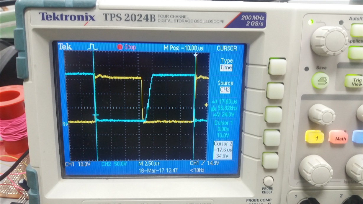
I am working on a two switch forward converter using UC2844A ,Converter Specs are input universal input voltage 90-264VAC,Output 450V DC @350mA. in this power transformer is heating and drain to source voltage of the MOSFET during turn off time is like ramp wave form,not as square wave form, let me know what may be the reason for this?

  • Sharathkumar,
    Thanks for your interest in TI here.
    It's difficult to say right now without a little more details. Could you post a schematic , transformer details , and images of what you are seeing? Note the "rich text editing" option in your reply where you can attach items.
    Regards
    John
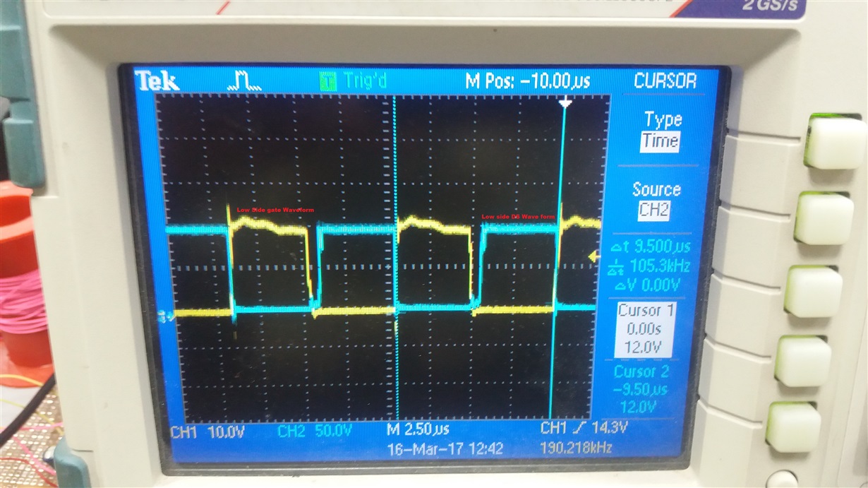
  • Blue is gate wave form and yellow is drain waveform 

    Transformer is ETD 34 with 56 primary turns and Secondary 272 turns divided into two sections 1376,and 10turns Auxiliary winding.

  • Hi Sharathkumar,

    Thanks for your reply, we will need your help to conduct few more tests in order to find the root causes of the problem.

    We are suspecting the body-diode of the low side MOSFET was conducting somehow right after the gate on-time as the Vds level fell slightly below the gate on-time level, this might due to the secondary diode is shorted or in backward bias. 

    Could you remove D13 & D16 and test the system with open loop to see if the primary waveforms improve? If the primary side waveforms look good without the secondaries involved, then add the secondary diode back one at a time to see if it makes any change. You might need to confirm the polarities of the secondary windings to ensure both rails are in phase as well before you put the diode back on.

    Also it would be helpful if you can provide higher resolution of waveforms and schematic, the ones you updated were a bit blur and it kind of hard to read the figures.

    Thanks!

    Best Regards,

    Wei-Hao

  • i checked the transformer secondary voltages,the polarity is correct only.

    today i observed the PWM frequncy is changing? may i know the reason it? actually controller is a fixed frequency one why the frequency is changing? i am suspecting because of control loop is it correct?

    can i use the two switch forward converter for 450V DC from Universal input?

  • Hi Sharathkumar,

    Thanks for your reply.

    The frequency jitter could be caused by the high voltage noise spike when the power switch turns off. The spike will couple to the oscillator RT/CT terminal and a spike of sufficient amplitude could prematurely trip the oscillator which caused variation in the switching frequency. I would suggest you to increase your CT capacitance greater than 1000pF and reduce the RT value accordingly to minimise the effect of noise spike.

    Could you please provide the primary side waveform after you remove the secondary side diode? is this problem been resolved yet?

    Thanks  

  • thanks for the reply i am sharing the waveform here in this  blue one is secondary side transformer wave form and pink one in primary side with no load and open loop testing...

    as you told for changing the value for RT and CT for fixing frequency constant tried increasing Ct value and reducing RT value but no effect.....

    do you have any design for 450V SMPS?

    is my design will work or not?i am problem stilll....


  • “Hi Sharathkumar,

    Thanks for your reply and unfortunately we do not have the high output voltage reference design that will meet your requirements. May I know what is your application?

    It is hard to tell where exactly the problem is, but there are some potential problems based on the information we have so far:

    1. You had placed a DC blocking capacitor C41 on the primary side of the high side gate drive CT circuit, but there is no DC restoring capacitor on the other side of the transformer. This may cause an issue because the high side FET Q1 might not be able to turn on and off properly. I would suggest you to place a same value DC restoring capacitor to ensure the high side FET is properly driven during the operation.

    2. The ringing on the secondary side waveform indicates the inductance of the X’FMR is resonating with the winding capacitances, this suggests the inductance of the transformer might be too high. The resonance frequency will reduce after you place the secondary side diodes back due to the contribution of the junction capacitance of the diodes, and that could be one of the reason why the drain to source voltage is slowly ramping up during the FET off time. Also the reason behind transformer gets hot could be the large winding resistance due to a phenomenon called proximity effect.

    Could you please let us know the inductance and leakage inductance of your transformer? You might need to redesign your transformer by reducing the number of turns to reduce the inductance and the winding capacitance.  Also, interleaving the windings will help reduce proximity effect losses, if your transformer is not already interleaved.

    Also can you show us the waveform for the switching frequency is changing? What is the value of your CT and RT right now?

    Thank you.

    Best Regards,

    Wei-Hao Chen

  • Hi Thanks for the reply,

    i am using ETD 34 Core and Primary having 47 turns and secondary having two sections with 117 turns and primary inductance is 6mH,leakage 22uH, winding pattern is first primary then secondary winding last is bias winding.

    present my RT is 10K Ct is 820pF,

    the above wave forms are at different AC input voltages yellow is gate wave form and blue is drain to source wave form.my bias winding voltage is coming more than the designed value and it crosses the maximum value of IC Vcc voltage this is causing the problem of frequency changing,i am suspecting....is it correct..

  • Hi Sharathkumar,

    Thanks for your waveforms, I am having some confusion here would you mind clarify them for me?

    1. You stated earlier, "Transformer is ETD 34 with 56 primary turns and Secondary 272 turns divided into two sections 1376,and 10turns Auxiliary winding" and in the most recent post you said: "i am using ETD 34 Core and Primary having 47 turns and secondary having two sections with 117 turns and primary inductance is 6mH,leakage 22uH, winding pattern is first primary then secondary winding last is bias winding.". Which one is the correct one?

    2. The waveform you have provided does not have the slow ramp for VDS? Does the DC restore capacitor help? What was the test condition i.e. loads, input, output?  

    3. I am suspecting the frequency variation was caused because the internal regulator for VREF was burnt due to your auxiliary winding voltage exceeded the maximum VCC rating. 

    Can you measure the auxiliary winding waveform as well as the VREF pin voltage under different AC input? The maximum rating for the VCC pin is +30V, the device will be damaged if you exceed this point.

    You can try to remove R33 & R35 and use the DC supply to apply external bias to VCC pin at a fixed voltage, and see the variation in switching frequency under different input voltages.If the switching voltage does not change after the external supply is applied, it could suggest the internal VREF regulator of the device was damaged due to your VCC exceeded the maximum rating.

    Thanks a lot.

  • 1 initially i designed for E32 transformer but manufacturer made same turns for ETD 34 i.e 56 one then i recalculated for ETD34 then arrived 47 so second one is correct...

    2  the test condition is 4k load and input 70VAc Output 440VDC

    3 2 to 3 times ic got damaged and changed with new ic also same problem...today i fixed the frequency changing issue by adding voltage regulator in series with then voltage is regulated then frequency changing is not happened,converter output voltage stable at 440V but if i  increase the input voltage getting noise from transformer and duty is not varying and pulses are oscillating... 

  • Hi Sharathkumar,

    Adding the voltage regulator solved the frequency variation problem indicates the aux winding voltage was too high which damaged the internal VREF regulator and I suggest you to reduce the turns ratio to ensure the VCC rating is not exceeded.

    When you say noise from transformer, do you mean you can hear the audible noise or you saw ringing on the waveform? I am not entirely sure about what do you mean by pulses are oscillating, could you please show us the waveform for Vout, DRV, VDS, and secondary winding voltage under high vin with no load and heavy load conditions.

    Thank you