This thread has been locked.

If you have a related question, please click the "Ask a related question" button in the top right corner. The newly created question will be automatically linked to this question.

TPS40057: TPS40057

Part Number: TPS40057
Other Parts Discussed in Thread: TPS40050-Q1

Hi  all ,

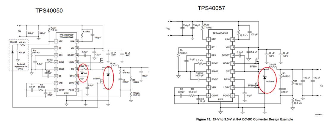
For a design of a 12V to 5V synchronous buck  the customer is using the “Tps40057 synchronous buck controller”.  

When comparing it to previous controller they were using “Tps40050-q1”.

the see that in both the applications and specs are similar.


1. Why are there differences with regards the diode application? (see below)

2. Do they need to add “D2” to their tps40057 application?


  • Hi Ariel ,

    Lets take both the usage of diode separately.

    1. Optional diode parallel to low side FET : During the dead time periods, the inductor current flows through the lower FET’s body diode. This
    body diode usually has a very slow reverse recovery characteristic that can adversely affect the converter’s efficiency. An external Schottky diode can be placed in parallel with the low-side FET to shunt the body diode and prevent it from affecting the converter’s performance. The added Schottky can have a much lower current rating than the diode in a nonsynchronous buck converter because it only conducts during the small dead time (which is typically less than a few percent of the switching cycle) when both FETs are off.

    2. Rsw and D2 on Switch node :The SW node of the converter is negative during the dead time when both the upper and lower MOSFETs are
    OFF. The magnitude of this negative voltage is dependent on the lower MOSFET body diode and the output current which flows during this dead time. This negative voltage could affect the operation of the controller, especially at low input voltages. Therefore, a resistor (between 3.3 Ω and 4.7 Ω ) and Schottky diode must be placed between the lower MOSFET drain and pin 12, SW, of the controller as shown in Figure 15. The Schottky diode must have a voltage rating to accommodate the input voltage and ringing on the SW node of the converter.
    Base don the layout , if extreme negativie ringing greater than 2.5V are seen on SW node then the clamp resistance and diode is recommended for both devices .

    ---Ambreesh
  • Hi Ambreesh ,

    Thank you for the elaborated answer.

    Further small closing details :

    1. “This negative voltage could affect the operation of the controller, especially at low input voltages”
    Can you please explain why negative voltage is bad here?
    2. I see that for D2 diode that is recommended is a “BAT54”.
    Can the “BAT54” fit also to the optional diode ?

    Best regards ,

    Arik.P.
  • Hi Ariel,

    You can use any diodewith Vrrm equal to Max input and about 0.5A Io current .
    As far as negative voltage is concerned , at lower input voltage because of higher peak currents you will see even higher ringing .

    ---Ambreesh
  • Hi Ambreesh ,

    www.onsemi.com/.../BAT54LT1-D.PDF

    Would this one be good enough?
    This is BAT54 as recommended, but Max current is only 300mA ...
    You stated 500mA.

    BrR ,

    Arik.P.
  • Hi Ambreesh ,

    Any update ?

    Best regards ,

    Arik.P.
  • The diode(BAT54) chosen should be fine .

    --Ambreesh