This thread has been locked.

If you have a related question, please click the "Ask a related question" button in the top right corner. The newly created question will be automatically linked to this question.

LP2953: Error Amplifier Specifications

Part Number: LP2953

Hello,
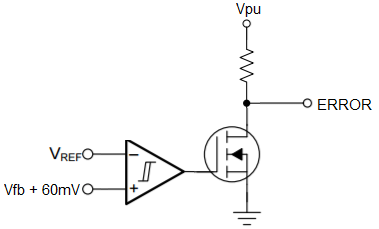
I would like to get some information about the LP2953 device, and more precisely about the Error Amplifier.
Could you, please, give me the Error Amplifier specifications (open loop gain, unity gain bandwidth, phase margin, input offset voltage) in the LP2953 ?

Thank you for your consideration,

Sincerely,

Aymeric

  • Hi Aymeric,

    Unfortunately these are not specs that we give out directly to people for competitive reasons. However, you can estimate most of them pretty easily. 

    • Open Loop Gain: roughly equal to the low frequency flat portion of the PSRR graph
    • Bandwidth: This can usually be estimated by taking the PSRR graph and finding the point where it starts to roll off, continue this line all the way to zero to get an approximation of the bandwidth. 
    • Phase Margin: Perform a load transient and count the number of times it rings, the more rings the less phase margin. See Section 5 in the application report AN-1733 Load Transient Testing Simplified for some comparisons for the number of times it rings and the measured phase margin. 
    • Input Offset Voltage: Measure the reference voltage (using a high impedance DMM), measure the voltage on the feedback pin (or the output if in unity gain). The difference between the two measurements is the total offset, this is the closest you can get as there is no way for you to externally measure the output of the error amp. 

    -Kyle

  • Thank you so much Kyle for your answer. I am trying to understand the schematic based on the block diagram (it is for my research).

    1) Based on the block diagram, the input V+ of the Error Amplifier is tied to -60mV (instead of its output with resistances...). Could you please tell me where does the bias come from?

    2) On the schematic, I can see that the output of the EA is the Q26 transistor, but what is the purpose of the Q29 transistor and the resistance R21 (4ohm)?

    3) Regarding all comparators, the output is either 0V or 5V?

    Thanks for your time,

    Aymeric

  • Hi Aymeric,

    See my answers below:

    1) Based on the block diagram, the input V+ of the Error Amplifier is tied to -60mV (instead of its output with resistances...). Could you please tell me where does the bias come from?

    The + input for the EA isn't tied to -60mV, instead the + input for the dropout detection comparator is set +60mV above the Feedback node (which is the tap point of the resistor divider used to set the output). During regular operation the feedback node is equal to the reference voltage (1.23V), however when the device starts going into dropout the feedback node decreases. If the feedback node drops by 60mV (5% of 1.23V) then the dropout detection comparator flips the ERROR signal from high to low.

    2) On the schematic, I can see that the output of the EA is the Q26 transistor, but what is the purpose of the Q29 transistor and the resistance R21 (4ohm)?

    While I'm happy to help you understand the general ideas behind how this device operates, I don't think I should delve into the specifics of the transistor level operation out of respect for your research project. 

    3) Regarding all comparators, the output is either 0V or 5V?

    The outputs of all the comparators are open drain topologies, see the schematic below. This means that the comparator drives a FET connected to the output pin. So when the ERROR pin is in a logic low state the FET is fully turned on and will equal approximately 0V (see figure 22 for the current carrying capability of that FET). When the ERROR pin is in a logic high state the FET is turned off and will be approximately equal to the pull up voltage labeled Vpu (the FET does have a small amount of leakage current, Ioh, which will cause ERROR to be slightly less than Vpu).

    -Kyle