This thread has been locked.

If you have a related question, please click the "Ask a related question" button in the top right corner. The newly created question will be automatically linked to this question.

LM1117: verify the layout of LM1117MP-3.3/NOPB

Part Number: LM1117

Support Path: /Product/Help with Device Selection/

Hello sir,

we are manufacturing product for automotive industries.

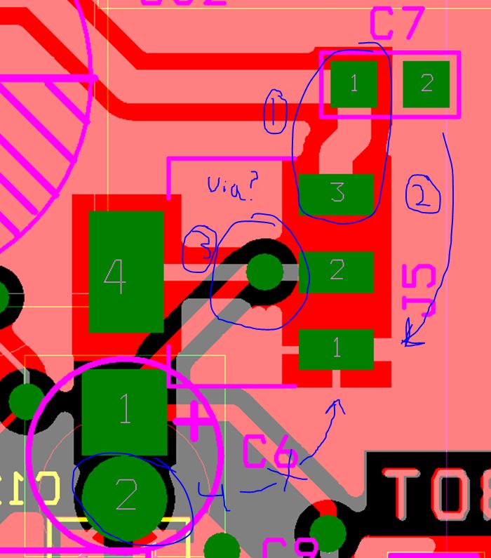
we would like to verify the layout of LM1117MP-3.3/NOPB

here we attched layout as well as ckt for your refereregulator 3.3v.docxAudio Controller V1.1.pdfnce

  • Hi Ravindra,

    I do not see your output capacitor in the layout you provided.  This capacitor should be as close as possible to the OUT pin and have a same layer connection to the GND pin (do not drop the ground side of the capacitor through a via).

    Very Respectfully,

    Ryan

  • Dear sir,

    thanks for prompt reply.LM1117 IC regulator layout updated.docx

    we made correction in our layoy ,

    please  go throught it once and confirm correction.

    PFA

    regards,

    Ravindra

  • Hi Ravindra,

    There are a few comments on your board with the output capacitor placement that would improve your application performance. Below I marked and numbered a few points.

    Your input capacitor placement and routing is exactly correct for a capacitor placement with regards to an LDO:

    1) C7 is placed close to the LDO pin on the same layer as the LDO and does not need to go through any vias.

    2) The ground side of C7 has a same layer (no vias) path to the GND pin of the LDO.

    While the placement of C6 may be adequate for your application, in general the same principles you followed for C7 apply to (and are generally more important) for the output capacitor, C6:

    3) It appears you drop though a via before the output capacitor. Vias add extra inductance and resistance into the loop. Ideally you would have a same layer connection such as you did for C7 (1).

    4) There does not appear to be a same layer ground connection for C6 to the GND pin of the LDO. Again this will add extra inductance and resistance into the loop. Ideally you would have a same layer connection such as you did for C7 (2).

    Very Respectfully,

    Ryan