This thread has been locked.

If you have a related question, please click the "Ask a related question" button in the top right corner. The newly created question will be automatically linked to this question.

TPS22968: Dual voltage inputs at different voltage levels; one voltage output design

Part Number: TPS22968
Other Parts Discussed in Thread: TPS22912C, TPS22910A, TPS22918, TPS22953

Hi,

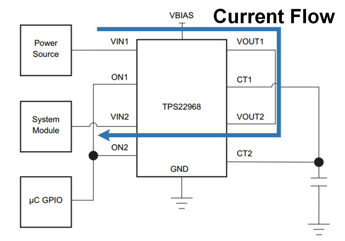
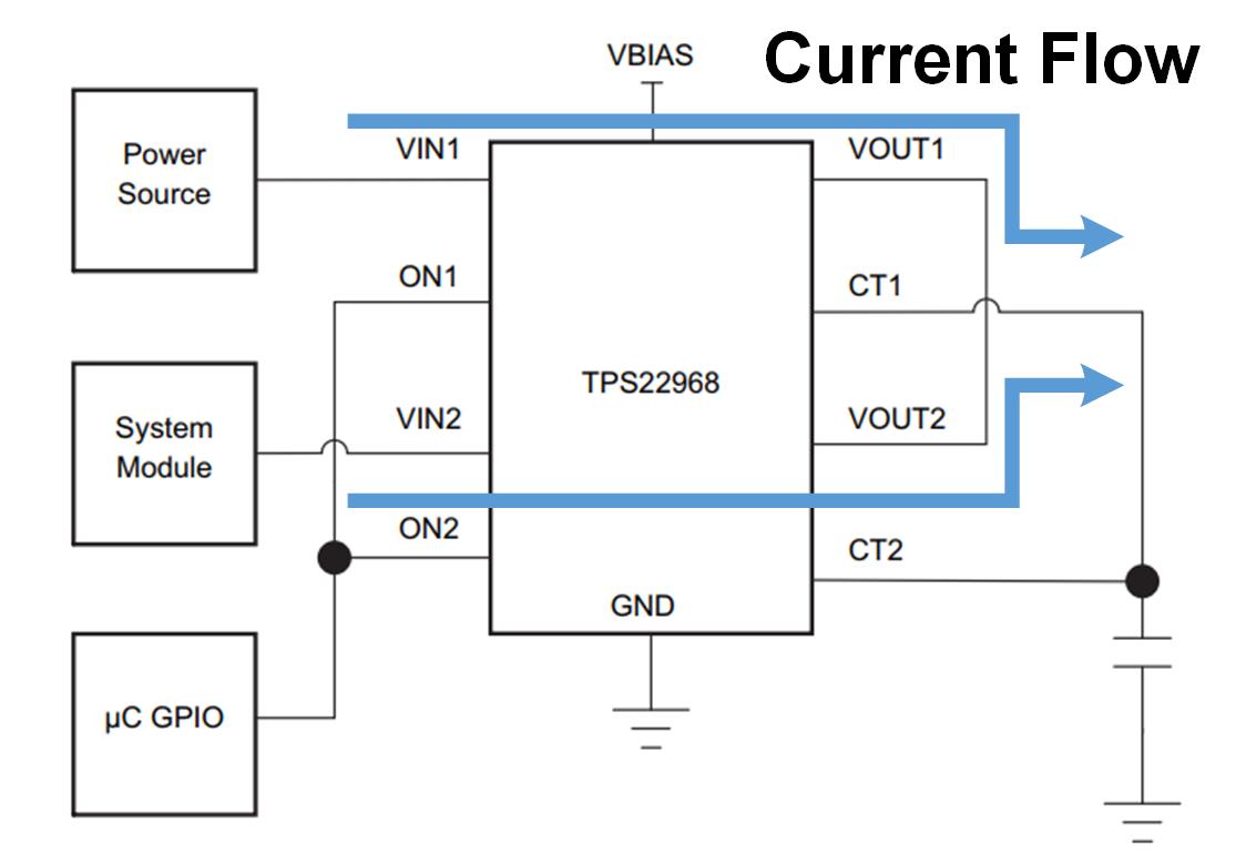
On page 19, Figure 34 of TPS22968 datasheet, what happens if VIN2 is at 0V via a pull down resistor to the ground? VIN1 is supplied with +5V, and CTRL sets VOUT = VIN1 through ON1, but ON1 logic comes from VIN2, and VIN2 is connected to ON2 then a pull down resistor to the ground. Is there any reverse current flowing to VIN2 in this situation? I need to use VIN2 as a voltage detection to switch the output to VIN2 whenever there is voltage present at VIN2. When VIN2 is left open and if there is reverse current, charge could build up and invert the logic and stop VIN1 connect to the output.

Thanks

  • Hi Hong Pan,

    If my understanding is correct, then you are using the TPS22968 for a power muxing configuration, where you have VIN1 supplying the output (VIN1=VOUT) and VIN2 is disconnected. When VIN2 is connected, you would like the device to stop supplying the output with VIN1 and use VIN2 instead.

    The problem with using the TPS22968 for this configuration is that it does not have reverse current built in. That means that if VOUT>VINx, current will flow backwards through the body diode. The leakage from VOUT to VIN2 will not be controlled, and there is a possibility that VIN2 will rise in voltage.

    On top of that, the TPS22968 has QOD, and this will be a constant drain on the output while one of the channels (VIN1 or VIN2) is off.

    For more information on power muxing, you can take a look at the application note here. What is the amount of current that the output needs? Also, can the output voltage drop when switching between VIN1 and VIN2?

    Thanks,

    Alek Kaknevicius

  • Hi Alek,

    You're correct that I am planning to use TPS22968 as power mux. On page 19, it says it has the ability to block reverse current, but it did not explain how to achieve the current blocking in detail, and on page 14, the block diagram does not seem to have reverse current capability. You brought up a good point about the QOD, but the datasheet says TPS22968N does not have QOD. That's why I wasn't concerned about QOD.

    If I understand you correctly, you're saying that TPS22968 does not have reverse current blocking capability when two input voltage are not equal? Would you consider having someone to revise the datasheet to make it more clear?

    The output current requirement for my application is only 0.2 to 0.5A. Voltage is switching between 1.65V and 5V, the voltage drop is about 3.35V, and one of the power rails could have its voltage removed. Reverse current blocking and voltage different between the two rails are my main concern. I read through the application note that you provided, it's been very helpful. Combination of TPS22910A and and TPS22912C seem like a really good solution. It has been talking about reverse current blocking and under-voltage lock out throughout the datasheet until page 20, in section 11.1.4, when it talks about output capacitor, it says when the system power is removed, reverse current could flow from output to input. Does it mean that the minimum voltage of 1.4V must always be present if reverse current blocking feature is needed?

    You comment has been very helpful, and the main reason I am looking at TI's load switch is because TI has done an exceptional good job at introducing how the load switch works with step by step detailed explanation and comparison against discrete ICs solution. I hope TI will continue to do it this way for all other parts.

    Thanks

  • HI Hong Pan, 

    I'm the applications engineer working on power muxing applications, thank you for kind feedback!

    To answer your question about the TPS22968, the device does not have internal reverse current blocking on each individual channel. However, reverse current blocking can still be achieved, but only if you follow the configuration shown on Figure 34, page 19. If you look at the functional block diagram for the TPS22968, you can see that each internal FET contains a body diode that faces from Vout to Vin. If you connect both channels in the configuration on Figure 34, this allows the body diode on the 2nd channel to block any reverse current flowing from VIN2 to VOUT2. 

    Regarding the question about the TPS22910A and TPS22912C, there are a few parts to the question that I would like to address. As you described above, there are some interesting scenarios that arise when one of the voltage rails are removed. 

    1: If the first load switch enable is off, VIN1 is at 0V and VIN2 is at 1.65V, the switch will work normally. The reverse current blocking feature will be applied on the first switch, and VIN1 will be protected. 

    2: If the first load switch enable is on, VIN1 is pulled to 0V and VIN2 is at 1.65V, the switch will also work normally. The reverse current blocking feature will be applied, and VIN1 will be protected. 

    3: If VIN1 has it's power rail removed, and VIN1 is left floating, then VIN1 will try to match the voltage on VOUT. In this case, VIN1 will try to remain at 1.65V just like VOUT. There will be a little reverse current coming from VOUT, but it will be a minimal amount since VIN1 voltage is close to VOUT voltage, and the load switch has some inherit minimal resistance (micro-ohms). 

    So if VIN1 power is removed, then the reverse current blocking feature will be disabled. However, the voltage difference will be minimal and prevent major reverse current from flowing.  

    I apologize for the long answer, but I hope I covered all of the possibilities with you. Let me know if you have any questions!

    Thanks,

    Arthur Huang 

  • Hi Arthur,

    Thank you for the detailed explanation.

    1. I am pretty sure that TPS22968 cannot be connected in the way shown in Figure 34, Page 19. TPS22968N can be configured that way because it does not have OQD. Even if TPS22968N is hooked up that way, it only prevent backflow current when the voltage rails on both inputs are the same or differ less than the turn-on voltage of the diode; in addition, both voltages have to be present. Alek has made it clear. 

    2. Can you point out the source of the information in which you're confident saying that when TPS22910A and TPS22912C are disabled, and VIN = 0, VOUT = 1.65V, reverse current feature will be applied? In setion 11.1.4, it is suggesting that if Vout is greater than Vin when no voltage is present, reverse current is possible. . "A CL greater than CIN can cause VOUT to exceed VIN when the system supply is removed. This could result in current flow through the body diode from VOUT to VIN." It seems like with or without the system supply removed, reverse current is going to flow until some voltage is present at VIN to activate the reverse current blocking feature.

    3. Where did you find the information saying that if the power is removed, and VIN1 is left floating, VIN1 will try to match VOUT? This is important to my application because I use of the VINs to turn on and off the switch, and the VIN that controls the switch is the one that will be removed. 

    Thanks.

  • Hi Hong Pan,

    1: I think I misunderstood the configuration. I initially thought we were describing a single-channel solution, with the current going from VIN1 through VOUT1 and VOUT2 and into VIN2, as shown below:

    The TPS22968 can be configured to support the application shown above. You are correct about the TPS22968 not able to support a power mux configuration, as shown below. I believe your application is similar to the configuration drawn below.


    2&3: In another E2E post, Alek collected some data on this configuration. His scope shots and data can be found here . From the shots, we can see that VIN will follow VOUT with the enable turned off (device is active low) and no load on VIN. The reverse current will peak around 20mA for 50ns. 

    Also consider taking a look at this app note, called Reverse Current Protection in Load Switches. The examples in this app note address many of the concerns you raised, and the TPS22912 and TPS22910A offer blocking even when the switches are disabled, as shown on page 9 and 10.

    Thanks,

    Arthur Huang

  • Hi Arthur,

    Thanks for the information. It's very helpful.
    I looked at TPS22953, but it does not have reverse current protection when the load switch is enabled. The app note that you provided mentioned that TPS2291xx family provides reverse current protection while enabled. I looked around in digikey, most of them are wafer size chip. I am avoiding them because they're difficult to rework and solder manually, and I don't think TPS22918 has reverse current protection. Do you know any other chip that is similar to TPS22912 or TPS22910A , and do not have wafer size package?
  • Hi Hong Pan,

    I sent you a private message. We might have a solution, please message me at a-huang@ti.com.

    Thanks!

    Arthur Huang