This thread has been locked.

If you have a related question, please click the "Ask a related question" button in the top right corner. The newly created question will be automatically linked to this question.

WEBENCH® Tools/LM5005: My circuit isn't working, and VCC is only 3 Volts

Part Number: LM5005

Tool/software: WEBENCH® Design Tools

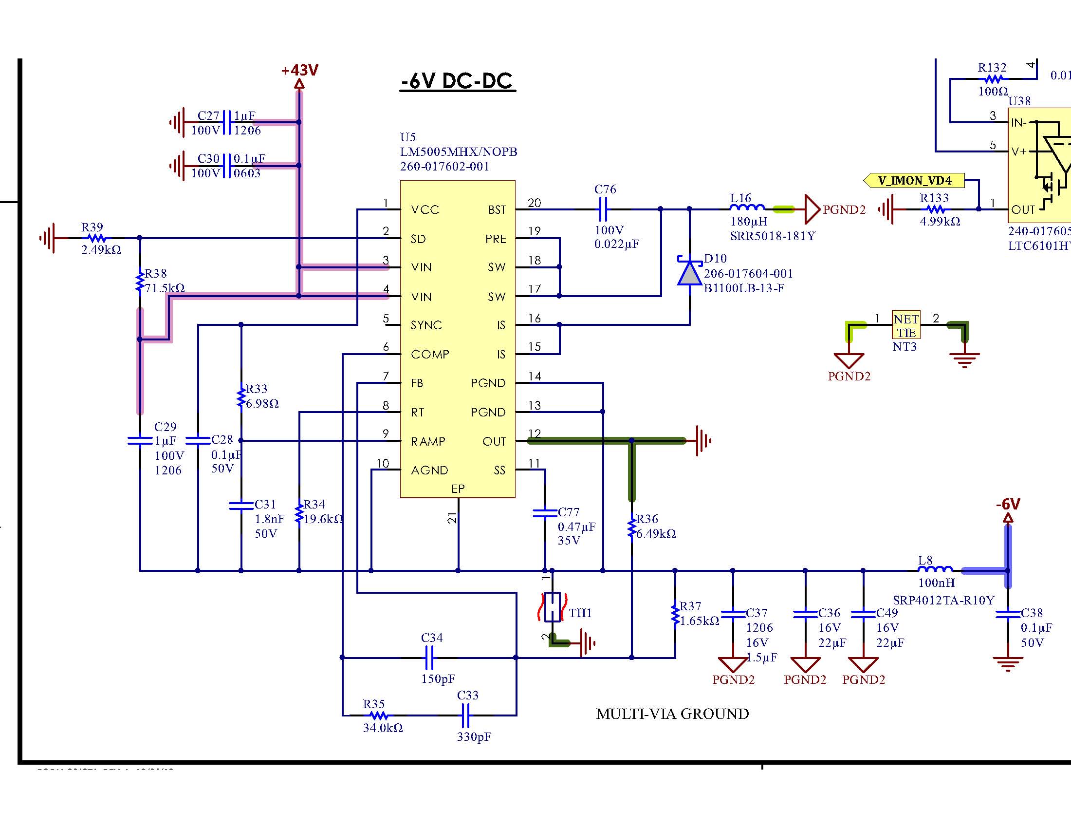
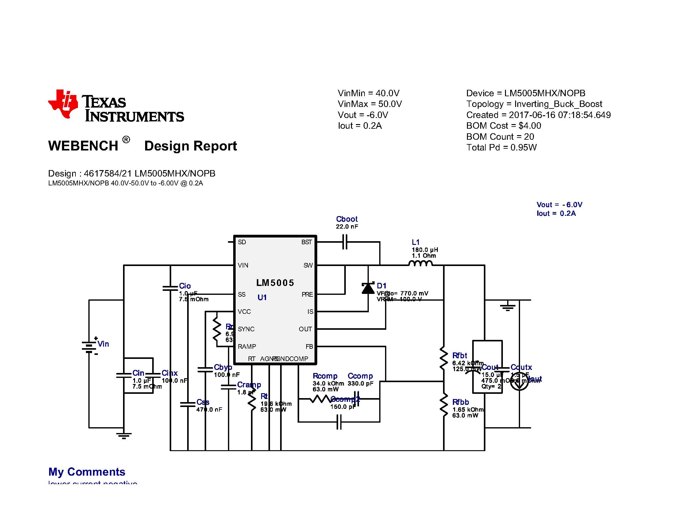
I'm not getting any voltage out of my circuit.  VCC is low (~3V) and I don't know why that is.  I'm attaching my schematic and the Webench report.  I have verified my SD pin is getting 1.4V from my voltage divider.

Any troubleshooting help will be most appreciated, I have verified my PCB does not accidentally have the EP node connected to Gnd.

  • Hello,
    From your post it is not clear if you are not getting any voltage on the output or just not getting desired voltage.
    Please make sure you have proper connections on the VIN, and check waveform on the switch node and voltage on FB pin.
    I would suggest checking following :
    1. input voltage and make sure your power supply is not current limited
    2. check switch node waveform and make sure device is switching when input voltage is present
    3. check voltage output node and verify if part starts up (output voltage rising or not)
    4. check voltage on FB node

    I hope this helps.
    Please let us know if you need further help.
    Regards
    Brani
  • Hi William,

    We think we found a major issue in the schematic. Can you please take out the R33 ramp resistor. It will load VCC into overload. If all is working and the part is switching then you can try to use a 1.4Mohm resistor instead of the 6.98Ohm you have in the schematic. But the ramp resistor is only needed when Vout is larger then7.5Vout. Please see the datasheet section "7.3.5 RAMP Generator" for more information.

    Another thing I would like to mention is that the SD pin comparator is IC internally referenced to AGND pin. So the bottom side resistor R39 of the input feedback divider is maybe better to place against AGND. A similar thing is probably with the high frequency decoupling caps C27/C30. These two caps may like to go from Vin pin 3/4 (connected the internal high side FET and the low side is referenced to PGND) to pin 13/14 in a low parasitic inductance path to reduce ringing.

    Third the VCC cap C28 and the BST cap C76 is a little bit on the low side. You may want to beef them up a bit to VCCcap=0.47uF and the Boot cap should be a X7R cap. Think about the capacitance de-rating over voltage and temperature.

    Please let us know if the circuit work now.

    Best Regards,
    Robert Loke
  • Removing R33 solved the loading problem on Vcc, but it still didn't have an output.

    Removing R38 & R39 solved the problem.

    Because of other circuitry present, I don't really need to worry about sequencing so I can live without the function of the SD pin.

    I'm happy my circuit is now working, but wondering why Webench recommended a 6.98 ohm resistor for Rramp.  I find it somewhat disconcerting that Webench recommended a value the datasheet calculations do not support.

    Anyway, all's well that ends well.  I don't need to re-spin the PCB and we can go forward with testing the rest of the PCB as well as our top level product.

    Thank you for the troubleshooting help.  I'm an RF Engineer by education and experience, but I was asked to do the power supply for this program, all 3 positive Dc-DC converters worked as expected, but the negative had issues. 

    Again, Thanks for the help.