Other Parts Discussed in Thread: TLV62585
Hi
Document No. SLVUB03
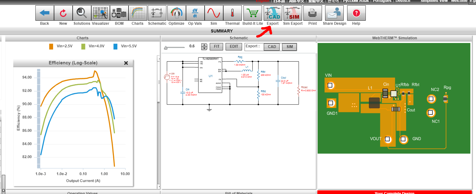
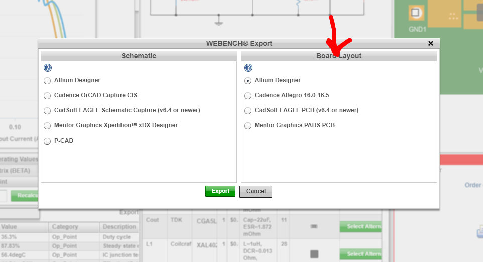
TLV62585EVM-824 Evaluation Module
As mentioned in the section “Board Layout”:
The Gerbers are available on The EVM product page: TLV62585EVM-824.
But I cannot find the gerber file in the link, could you please provide directly?
Thanks
Regards
Ben