This thread has been locked.
If you have a related question, please click the "Ask a related question" button in the top right corner. The newly created question will be automatically linked to this question.
Hi,
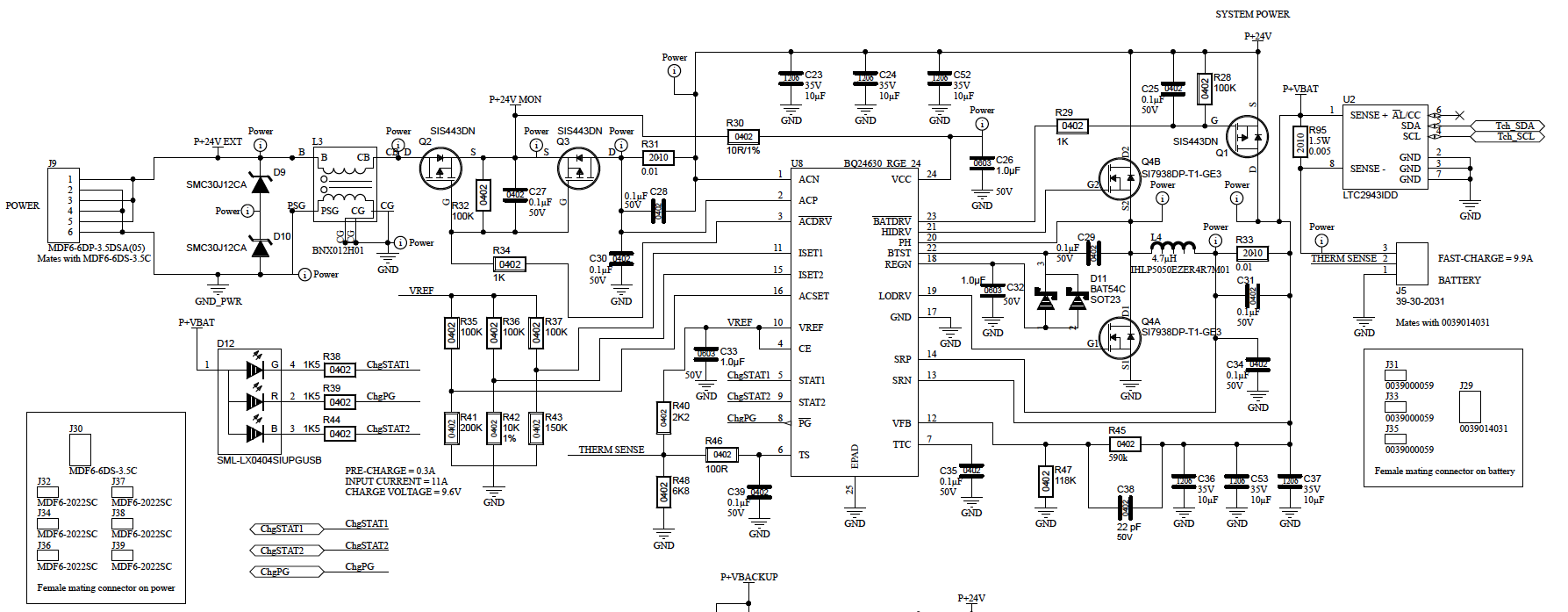
I have a design mostly based on the reference design for a 3S LiFePO4 battery.
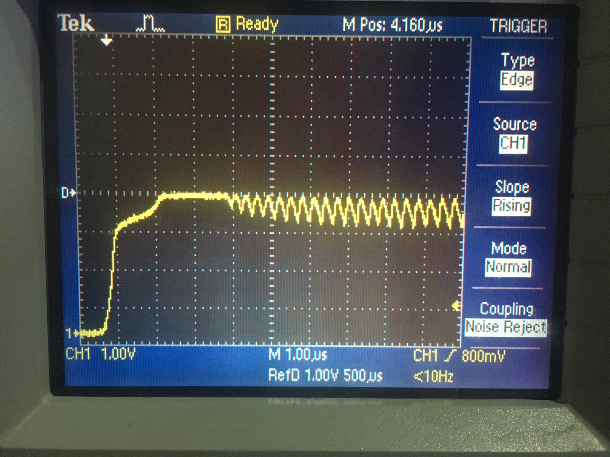
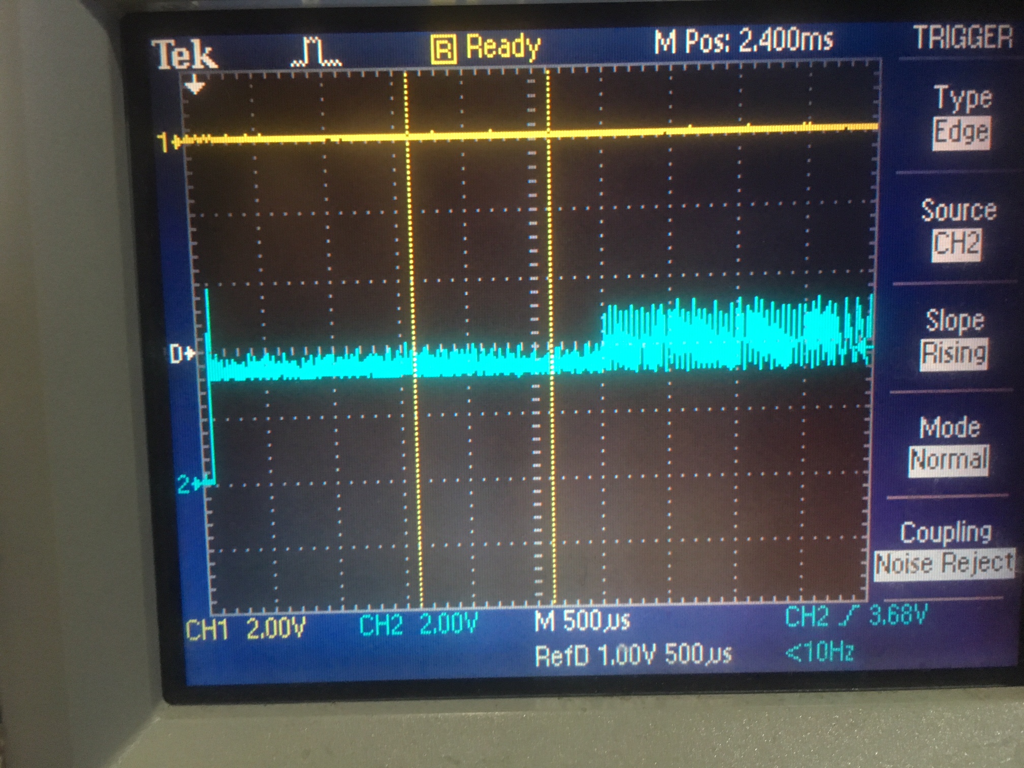
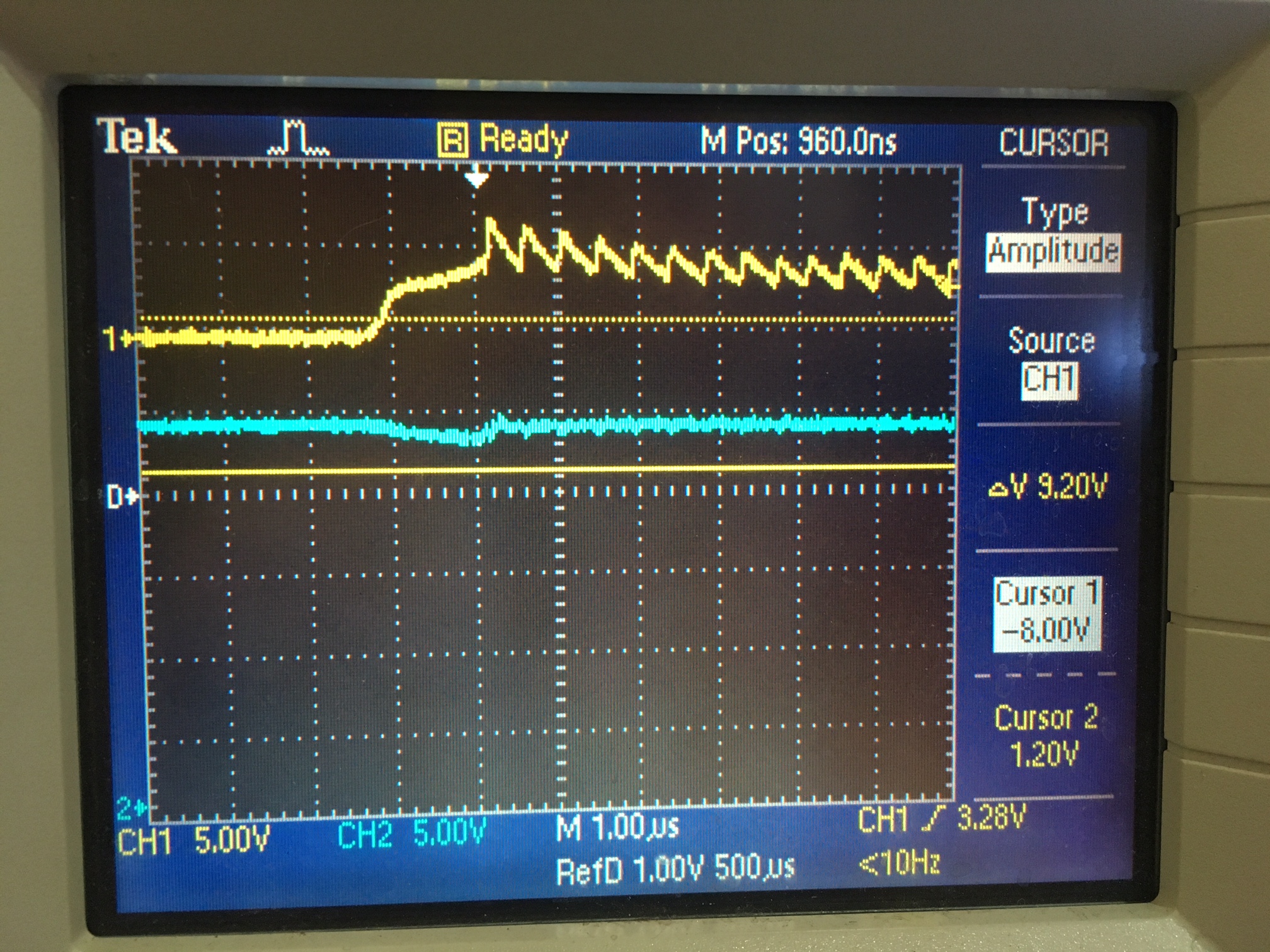
I apply 24V to the BQ (checked it on ACN/ACP and on VCC. Draws about 30mA on complete board, so not major fault but the charging does not function.
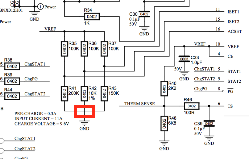
On closer inspection I measure that Vref is 4.076V instead of the 3V3 specified in the datasheet.
Any ideas why this would be the case?
Other measurements to be done to help resolve?
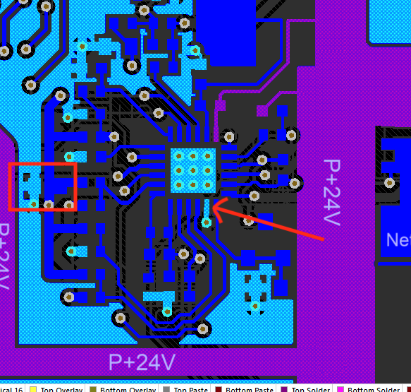
Schematic below/attached.
Thanks in advance
Ivor
I will captured the waveform of VRef and it is shown below the schematic. Vref is only used at the BQ to generate the setting values for ISET1/2, ACSET and the TS pin. Now where else it is used. The VCC signal rises very sharply to 24V and remains there. I did not save that waveform.
In the mean time I did find an error. See the redblock in the schematic below. The junction is missing, so two pins (R41 and R43) was not connected to GND. I have fixed that, but of course the reference is still wrong, so I will replace the chip again now that this error is fixed.
Jing, thanks for sticking with me to try and solve this problem.
As far as I can tell, the chip is not switching, i.e. no waveform on the inductor. Is that what you meant by switching? The Vref supply is an LDO,right? not a dcdc?
I also thought that ISET1 and ACSET should not have an effect, but not knowing the insides of the little black box, I thought I would just go ahead and replace it to rule that out as well.
I have thoroughly checked the VRef pin/trace for possible shorts to other nets but found none. The oscillation present on VRef does not seem to be present on any other pin of the device.
There seems to be about a 32ms delay from when 24V is applied (VCC) to when ACN/P is starting to rise. The signal on ACN/P is a good looking soft start curve to 24V.
Below are three plots of the Vref and VCC at 3 different sec/div values. The trigger is setup on VRef. Full bandwidth is used (it is a 2GS/s (200MHz) Tektronix). The oscillations on VRef are at 2.38MHz.
Jing, the PCB is a 4 layer board with ground and power internal layers. Below is snapshots of the area around the chip. The red arrow points to pin 17 for ground connection. It has via directly to ground plane right at the pin. The other picture is of the ground plane.
As you can see, the middle pad is also connected to ground with multiple vias.
I also just double checked pin 17 under microscope and it is soldered well. I cannot check the power pad, but it "should " be soldered ok after the reflow.
I also checked to make sure that the ground is not isolated by any means ( like a island in plane etc).
The GND I used was a little further away than I would have like, but now I measured it just over the cap. Below are the traces at different sec/div resolution. You will notice it is almost as if the chip is trying to regulate at 3V3 for 3ms but then gives up and goes ballistic.
Hope this can give you some new ideas. Can we skype chat about it, its a little more interactive and then we don't clutter the forum with all the screenshots.