This thread has been locked.

If you have a related question, please click the "Ask a related question" button in the top right corner. The newly created question will be automatically linked to this question.

UCC25630-1EVM-291: How to built in UCC25612-2

Part Number: UCC25630-1EVM-291
Other Parts Discussed in Thread: UCC24612-1EVM, CSD18536KCS, CSD18535KCS, UCC24612

Hi all,

UCC25630-1EVM-291 is full wave two Diodes Rect.

Many customer want to change Diodes to SRs.

But UCC24612-1EVM is expensive to buy.
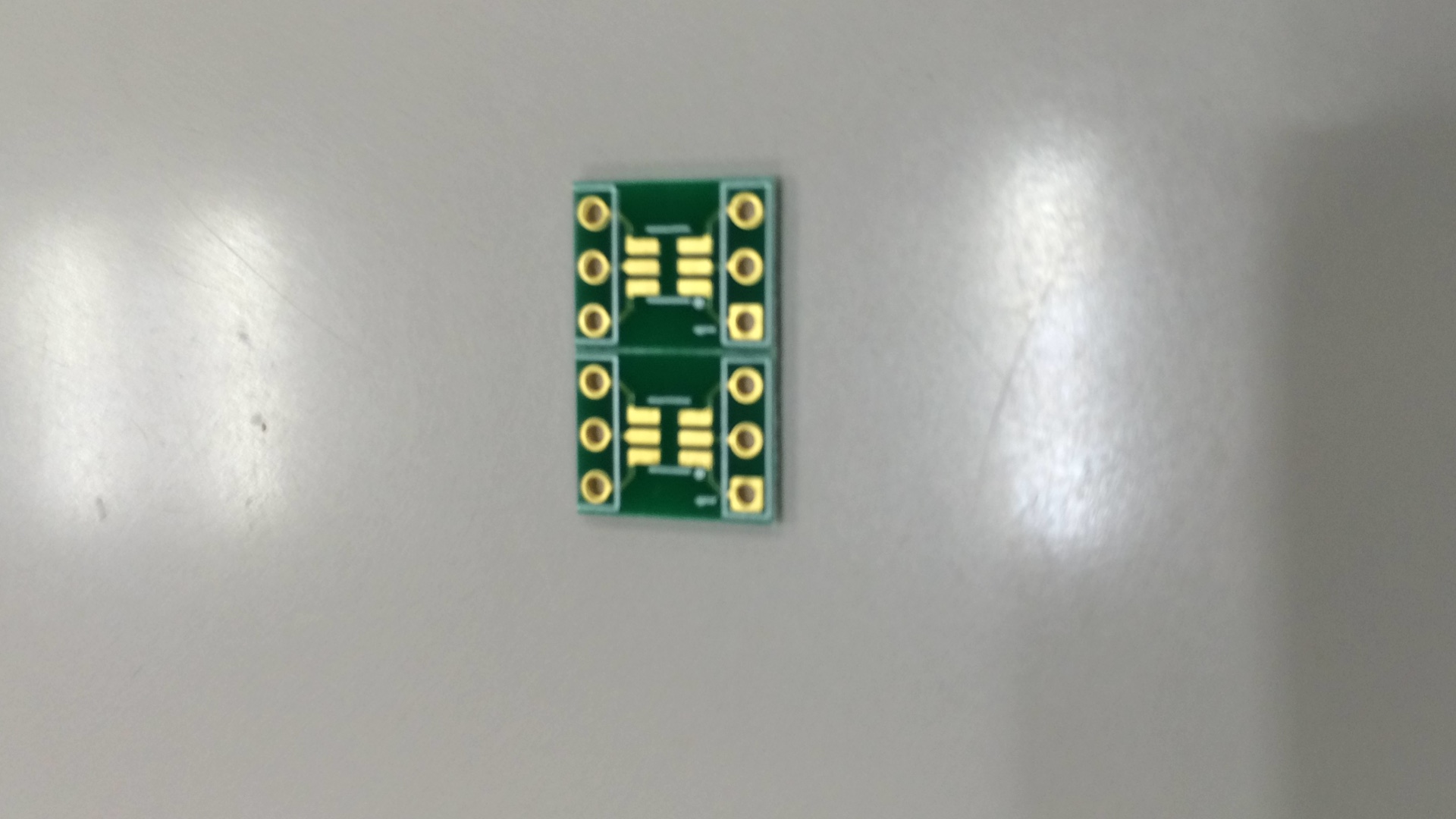
There are board which extension wire from SOT-23.

two CSD18535KCS or CSD18536KCS.
two UCC24612-2DBVT
extension board and wires. and some C, R
I do not want 1ohm resistor.

We needs circuit (cut and connect ) picture.
And caution for which wires should be short ( ? mm length )

Thank you,

H.DOI

  • Hi Hiroshi-san,

    You would need to configure each UCC24612 for high side operation as shown in this picture.

    The device requires a decoupling capacitor connected from VDD to VS and should be kept close to the IC. VD and VS should be connected as close as possible to the MOSFET drain and source respectively. 

    If you would prefer, I can send you gerber files of the UCC24612 EVM that you could use to build evaluation boards.

    Best Regards,

    Ben Lough

  • Thank you.
    But I do not want Hi-side rect. It is not good efficiency without aux.wire.
    This is efficiency challenge.
    I want Low-side rect. with modifying UCC256301EVM.
    No transformer change. No making new board, just use the picture board.
  • Hi Hiroshi-san,

    The transformer is configured where the center tap is connected to ground. You would need to disconnect the secondary side transformer pins from the EVM board. Pin 7 and Pin 12 of the transformer would need to connect to SR MOSFET drain. Each SR MOSFET's source would connect to ground. Pin 9 and 10 of the transformer would need to be connected to the output.

    Best Regards,
    Ben Lough
  • Ben-san,

    I understand.

    And now, Lo-side connection is like  TIDA-01557 Schematic.

    I think that   1ohm R6 , R15 and R17  are unnecessary in the case of hand-made cct, what do you think?

    Thanks,

  • Hi Hiroshi-san,

    R6 and R15 are used to slow down the gate drive signal to limit the amount of ringing on the MOSFET drain. R17 with C16 and C17 form an RC filter for the SR driver power. It is recommended to place an RC filter on the VDD pin at 1/100 of the max switching frequency of the converter. Having R6 and R15 are not necessary but will help limit the ringing on the MOSFET drains. If they are not used, you may need a more aggressive snubber circuit to keep the ringing below the Vds rating of the SR MOSFETs.

    Best Regards,
    Ben Lough