This thread has been locked.

If you have a related question, please click the "Ask a related question" button in the top right corner. The newly created question will be automatically linked to this question.

TPS61073: Certainly ESD issues !!!

Part Number: TPS61073
Other Parts Discussed in Thread: TPS61240

Hello,

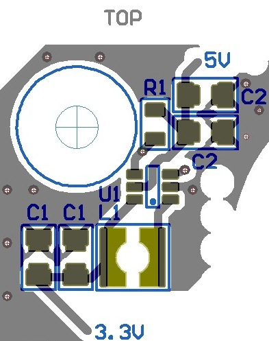
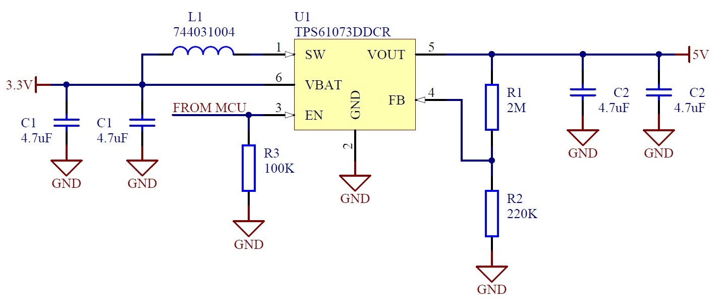
I am using TPS61073 IC as a 3.3 VDC to 5 VDC booster in adjustable mode with the feedback resistor values R1 = 2M, R2 = 220k.

I am enabling the IC using one of the micro-controller port with 3.3 V (same as input) supply through a pull down resistor of 100k (to avoid floating state). Please refer schematic below:

I was facing two issues in my design, detailed as:

1. IC heating up and emerging of fault condition (STILL NOT DETECTED WHAT EXACTLY HAPPENED INSIDE) in the IC resulting in output voltage = input voltage.

Corrective actions - I found that due to the pull down resistor value - 100k at enable pin the current consumption at enable pin was more than rated as per the datasheet.

I changed the pull down resistor value to 20M and limited the current to 0.16 uA which is now less than 0.3 uA as declared by the datasheet.

I understood that due to over current supply the problem occurred (Please correct me if I am wrong here). Secondly, I want to know what exactly got damaged inside the IC ?

2. The second problem which is still occurring is regarding ESD. As soon as I touch the area over 2M resistor and the output capacitors, the IC shuts down producing output voltage = input voltage.

 Corrective actions -  Currently I have no other option than potting the whole circuit. Please help me with some solution so that I don't have to encapsulate the whole circuitry. 

  • 1. please share TPS61073 layout image, the damage could be cause by the layout
    2. don't touch the 2M resistor. the IC may damage if you touch the FB pin, as the device doesn't have output over voltage protection function
  • Hi Jasper,

    1. Please check the layout images below.


    2. I understand that we should not touch the 2M resistor. What else can be done to avoid the problem. For me, the last option is to encapsulate it using potting compound. Do you have any alternative ?

    I have one more query, shall we avoid measuring voltage at feedback pin during functional assessment ?

    Thanks and regards.

    Sandeep Sati.

  • the layout is not good. for the damaged device, please measure the impedance between SW and GND pin. this help to check if the devices is destroyed by voltage spike in SW pin.

    yes. avoid measuring the FB voltage of TPS61073. another solution is TPS61240, which also support 5V VOUT without external feedback resistor
  • Hi Jasper,

    1. I measured the impedance between SW and GND pin. For damaged ICs, the value measured was 30 ohm and 5 ohm for two separate devices. For fresh ICs the value is 30 kohm.

    2. Can you please guide us for a good layout ?

    3. Thank you so much for the solution of TPS61240. We shall plan for this IC in the next revision of our circuit. Currently, we are using SOT23-6 package. Can you suggest any equivalent booster IC having 5V fixed output in SOT23-6 package ?

    4. Lastly, is it fine to use a resistor of 20 Mohm at Enable pin instead of 100k for pull down purpose (as described in point 1 of my initial reply) ?
  • 1. from the measure, the SW pin is damaged.
    2. you can refer to the user guide of the TPS61070EVM.
    3. there is not other solution with same package.
    4. it may be fine. need to make sure the EN voltage is lower than logic high voltage when there is leakage current from MCU.

    please try the two solution
    1. have a 10nF capacitor in parallel with the R3.
    2. measure the voltage spike in SW pin with minimum probe loop. then add RC snubber circuit between SW and GND, 330pF+6.8ohm.