This thread has been locked.

If you have a related question, please click the "Ask a related question" button in the top right corner. The newly created question will be automatically linked to this question.

TPS54386: Dual power supply, Vin 12V to Vout 5V & 3.3V design issue

Part Number: TPS54386

Dear sir,

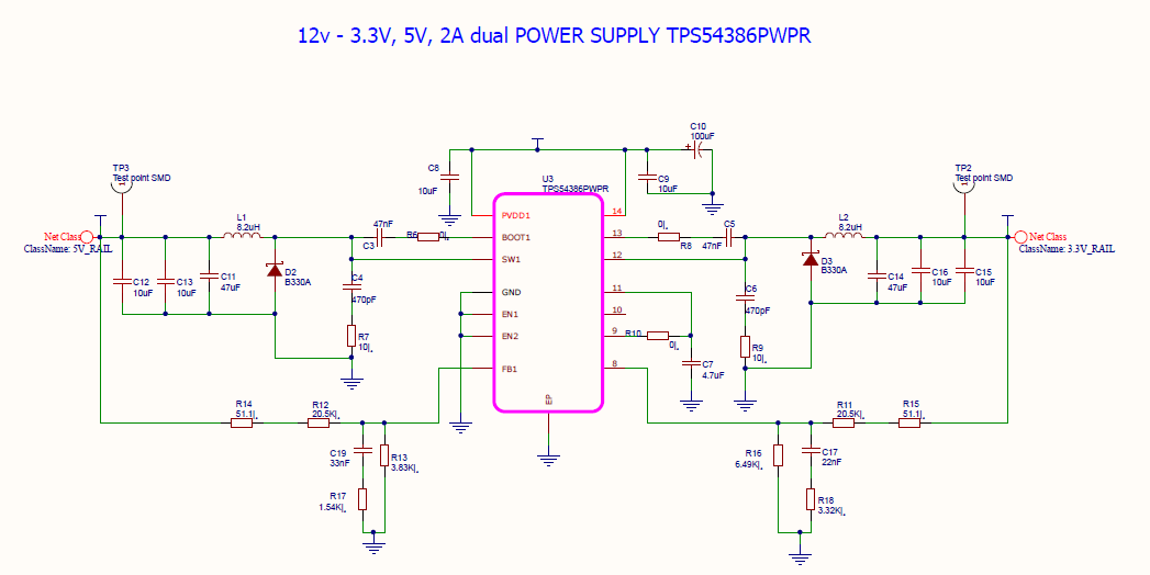
We are in the middle of designing a product prototype which uses TPS54386PWPR for a dual power supply, Vin 12V to Vout 5V & 3.3V with maximum load current 2A each. But we are facing a problem in getting output- 5V and 3.3V. instead, getting approximately,

2.4V @ 5V output side and

1.5V @ 3.3V output side

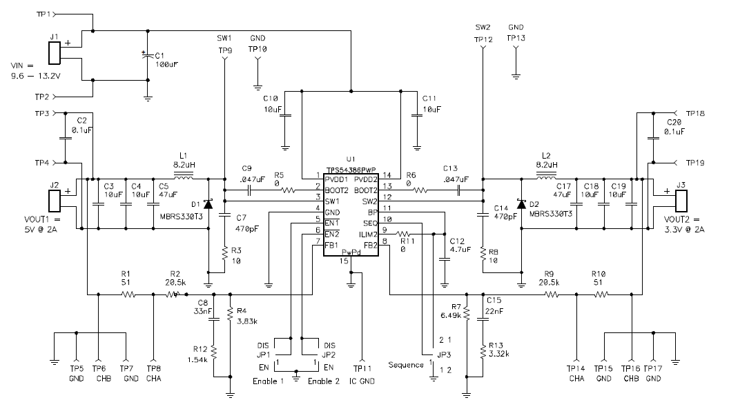
We have adopted the schematic diagram from TPS54386EVM user guide and also used ti design tool, in choosing components values, types, voltage rating etc. (with reference to the section in , TPS54386EVM user guide, page number 5. www.ti.com/lit/ug/sluu286/sluu286.pdf )

Test conditions:

1. Vin = 9.4V DC

2. SEQ left floating.

3. ENx, both are connected to GND.

4. Pin ILIM2 connected to pin BP

5. Diode is B330A-13-F, slightly different from reference design, but specification is (Peak Repetitive Reverse Voltage) Vrrm =30V Output current, Io =3A


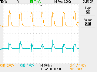
Please note down the observations on various test points(TP):

Output:

2.4V @ 5V output side (Very less than required voltage 5V)

1.5V @ 3.3V output side (Very less than required voltage 3.3V)


Voltage @ FB1 & FB2:

Voltages at FB1 & FB2 are not perfectly DC voltage of 0.79V , but Approximately 0.1V. Please note down the DSO images below for your ref.:


CH1(Yellow) : Voltage waveform @ Output 5V side,

CH2 (Blue) : Voltage waveform @ Pin FB


Please help us with your valuable feedback as we are unable to proceed further.

Sunil Kumar NK

  • Sunil,
    Please post your actual schematic. If you are using the identical schematic to the users guide with the above mentioned modifications, then you should get 5 V and 3.3 V outputs with a 9.4 V input. It looks like your supply is restarting. Since it is happening on 10 msec intervals, it is almost certainly hiccup current limit. Can you remove your loads and see if the circuit starts up properly?
  • Sunil,
    That is just the schematic from the users guide. I would expect you had to make your own schematic and PCB layout using your own CAD system correct? What are you using for printed circuit boards?
  • Dear sir,

    Thanks for your immediate response. Please find below schematic that we used in our application.

    As you mentioned, we have checked the output by removing the load. But no change to the waveform. We also checked and confirmed that,  there is no short circuits/ low resistances between Output & GND.

    Some additional information/ known errors in our pcb that may help you to find whether it may affect this issue or not.

    a) Input Capacitors are not closer to pins, PVDD1 and PVDD2 as per guidelines. Input capacitors are: CERAMIC CAPACITOR 10UF 10%10V X5R 1206

    b) We are using double sided PCB, and ground plane is applied on top of the PCB only.

    c) Is feedback circuit and other sections for this design are very sensitive to noise? (at the same time we will recheck the restarting behavior that you mentioned in previous reply.) 

    d) Track width of 12V supply rail is only 10mils,35 micron thick only (similar to all other tracks), and this is also different from layout provided in TPS54386EVM USER GUIDE.

    PCB Screenshot of TPS54386 - Dual power supply section:

    Thanks,

    Sunil Kumar NK

  • Sunil,
    With that PCB layout, I am not surprised you are having issues. I think you will need to follow the layout guidelines more closely to get your circuit to work. Long, narrow paths for the critical circulating current loops for the input and output will certainly cause problems. Please study the datasheet section 11 and let me know if you have questions about it.