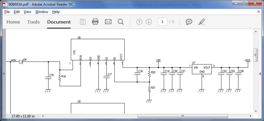
Two instances of failed regulators (U6: LMZ14203H) in the field or at customers facility. There have been no instances of U6 failing at our factory as of yet. This regulator is used in a total of 14 places in our product. There are a few differences between the implementations of each of the instances, but the key outstanding differences are the fact that the load on this part is very low (only about 180 mA), as well that the blocking diode D4 is used here to allow the M&C system to have power slightly longer than the rest of the system (from the 40 V bus) after loss of power. Values of components are per para. 8.2 of the data sheet. 
Regulators that are NOT failing are loaded at roughly 1000 mA and have slightly higher output voltages (13 pcs total in the same product and same environment).
Failure mode
The failure results in a gross short circuit from input to ground, as well as output to ground. No visual evidence of failure is indicated, and there are no signs of thermal distress (the conformal coating has not discoloured at all). This failure mode of the power converter also results in fusing of D4 due to over current.
Failure analysis
Investigative leads: The unique light loading of this instance of the power converter suggests that the input voltage may be subject to load dumps causing surges as a potential cause of failure. During switching, the commutation of the input circuit causes a di/dt charge of the input capacitor induced by the parasitic input inductance. It was thought possible that the input voltage was experiencing moments exceeding the input limit for this part (which is 43.5 V ).
Does TI have any advice as to why the parts are failing in this specific application and can you provide any recommendations? This is URGENT.
Regards,
John Lazar
Director, Product Development
669-275-2798

