This thread has been locked.

If you have a related question, please click the "Ask a related question" button in the top right corner. The newly created question will be automatically linked to this question.

BQ25703A: BQ25703A: CHRG_OK issue

Part Number: BQ25703A
Other Parts Discussed in Thread: BQSTUDIO

Dear Sir,

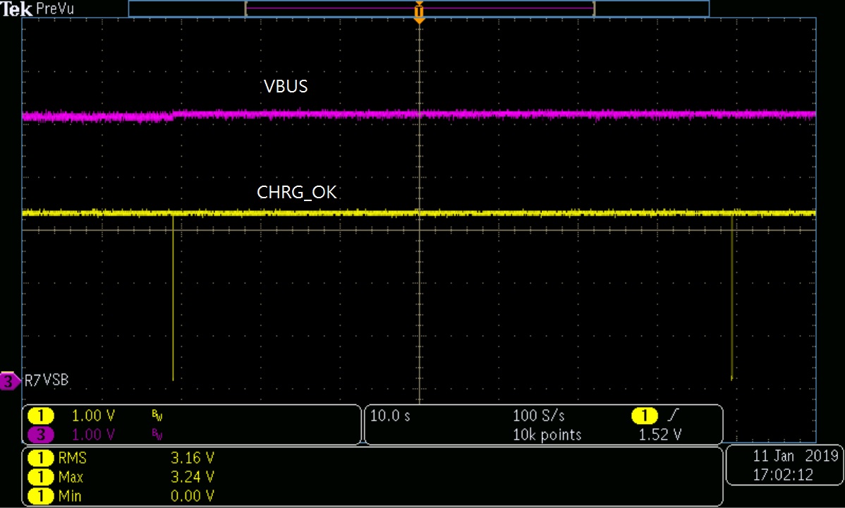
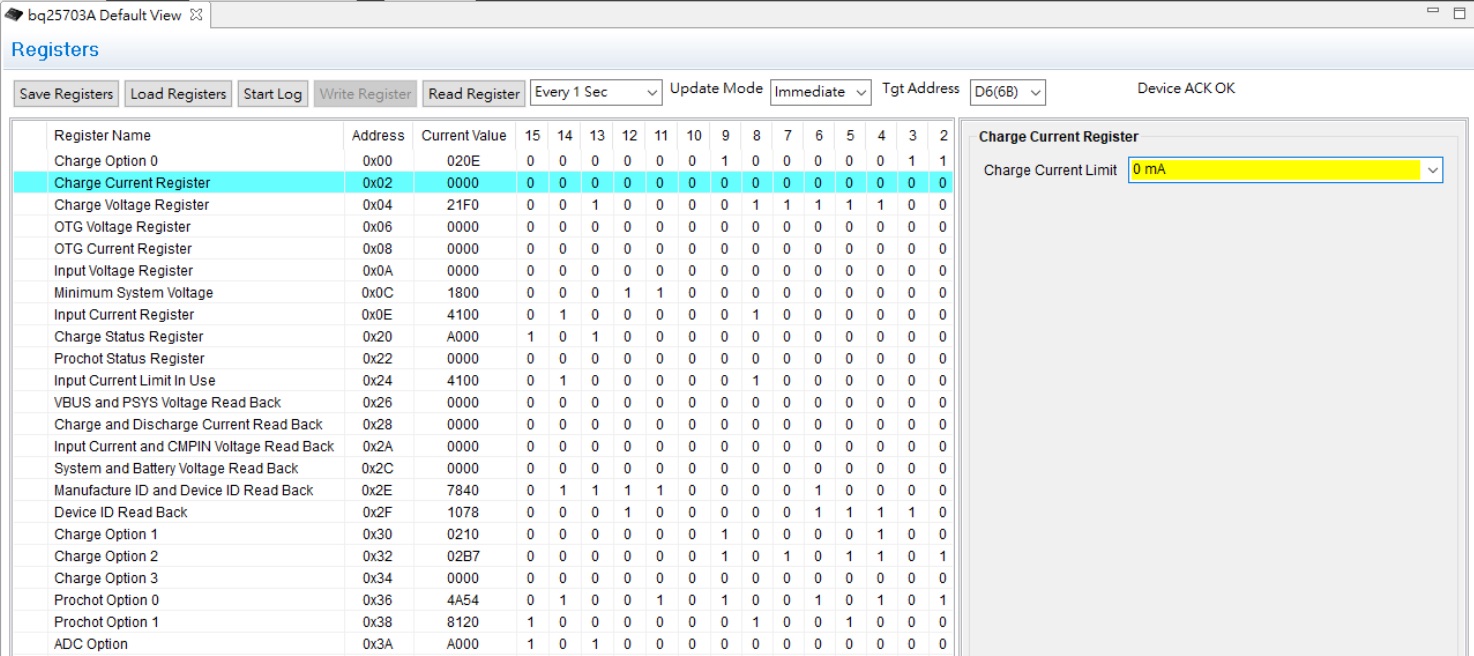
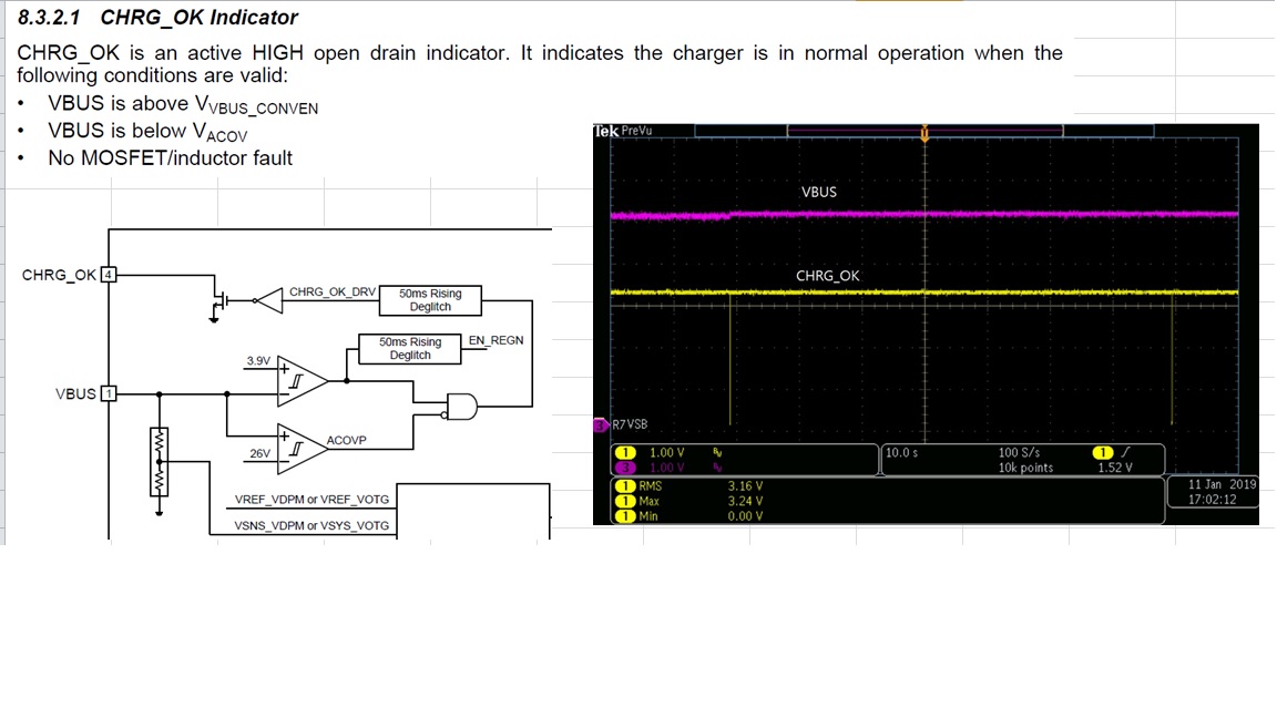
My customer have issue, CHRG_OK will drop.

I check below 3 condition didn't have happen:

• VBUS is above VVBUS_CONVEN
• VBUS is below VACOV
• No MOSFET/inductor fault

Could you advise what kind condition will make CHRG_OK drop?

Thanks!

Steven

  • Hi Steven,

    Please refer to the Functional Bloc Diagram on the BQ25703A datasheet Page 23 and the description on Page 7. The CHRG_OK state is determined by the VBUS voltage range and the pull up voltage source of this open drain output. Can you ask the customer to provide the waveform of CHRG_OK, VBUS and the pull-up voltage on the same screenshot when the CHRG_OK drops?
  • Hey Steven,

    CHRG_OK also goes low when a fault is active. You can find this in the pin functional description table.

    Can you provide a register dump of the charger, specifically from the Charge Status Register?

    Is there also some other event occuring here from a system side? This is a small window in time, but is the behavior also periodic?


    Regards,
    Joel H
  • Dear Joel,

    As you see waveform, VBUS didn't have any OV & UV.

    May I know what is " No MOSFET/inductor fault " ? as function block didn't have indicate any block.

    Below is my customer register table, please you kindly review & suggestion.

    Thanks!

    Steven

  • Hey Steven,

    From your BQStudio screengrab, I want to know if this was taken before or after the CHRG_OK pin dropped?

    Also, I had previously asked if this waveform you provided shows periodicity? In other words, if the CHRG_OK happening at a consistent rate? We can only see two events here, so I'm curious if this continually occurring.

    Can you also provide a schematic of the charging system to verify validity?

    Lastly, to your question about the MOSFET/inductor fault, these would be classified as the ACOC, ACx, and Q2 Overcurrent protections and this respective thresholds as listed in the Electrical Characteristics table of the datasheet.


    Regards,
    Joel H
  • Dear Joel,
    I want to know if this was taken before or after the CHRG_OK pin dropped?
    ->As you see waveform CHRG_OK have regular drop.
    About customer's circuit, I would provide another e-mail to you(please you kindly sent private mail to me).
    Thanks!
    Steven
  • Hey Steven,

    That does not answer my questions.

    Is this behavior periodic?
    Is register dump taken after the drop or is this just normal charge settings?

    I have sent you a private message to send the schematic to.


    Regards,
    Joel H
  • Dear Joel,

    Is this behavior periodic?
    -> I it some time will happen.
    Is register dump taken after the drop or is this just normal charge settings?
    -> normal charge setting.
    The circuit sent by another mail.
    Thanks!
    Steven
  • Hey Steven,

    After reviewing your schematic, the configuration of the input is incorrect. I will refer to the application diagram in the datasheet the example. 

    You will find that the larger input filtering capacitors are located before the 10mOhm RAC resistor. After the RAC resistor, there is a 10nF capacitor maximum placed between the ACN line and the drain of the HSFET1 (Q1). It is critical that the 40uF capacitance not be placed between ACN and the HSFET1 (Q1) drain. In your schematic, this is the case. 

    Filtering at this node can cause instability in the control loop which uses the differential voltage on this line to measure the inductor current. By filtering this, the measurement is filtered with each turn-on of the FET. This may likely be the cause of the issue in your design.

    Regards,

    Joel H