This thread has been locked.

If you have a related question, please click the "Ask a related question" button in the top right corner. The newly created question will be automatically linked to this question.

TPS61221: Vout not equal to Vin when EN pin is pulled to ground. Also, Vout ~2.8V instead of 3.3v even when EN is pulled high and load ~100mA

Part Number: TPS61221
Other Parts Discussed in Thread: TPS61020, TPS62730, TPS61097A-33, TPS61291, TPS61201

Hi,

Need your help.

While designing a low-power circuit for driving an at328p mc and a couple of sensors attached off a 14505 LiSoCl 3.7v battery.

BOM: 
NR3010T4R7M 4.7uH 1.02A, GRM188R60J106ME47J 10uF

Schematic (as in datasheet): Vin is connected to pin 1 of the switch on the top left.


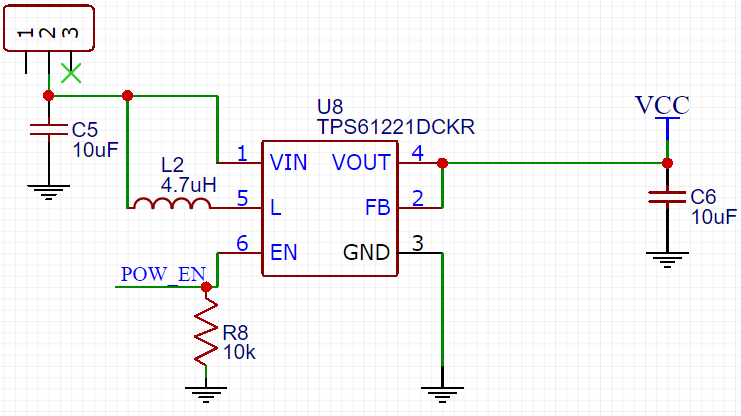
1. Vout should be equal to Vin when EN pin is pulled low. However, this doesn't seem to be the case in our experiments. We found Vout to be ~2.8V when Vin was ~3.5V. What could be the cause of this drop? 

Could this be caused by the output capacitor not being placed close to tps61221 as seen below? (It is actually located next to the Vcc pin of the microcontroller).

Would the following alternate layout help?

2. What happens if Vout is pulled to 3.3V (say by the an ISP programmer connected to the MC on the other side, Vout, of the tp61221) and Vin is not connected to any power source (isolated by a physical switch). Is this likely to result in some malfunction?

3. What if both Vin and Vout are connected to two different 3.3v supplies (battery, programming header)? EN pin is likely to be pulled LOW in these scenarios.

Thanks.

Anupam

GRM188R60J106ME47J
  • Hi Anupam:
    I didn't not understand your circuit condition clearly. What's the voltage range of Vin and Vout?

    For your detail questions:
    1# The voltage drop is caused by the diode mainly. Please see the function block in datasheet. and 10.3.2.:
    During shutdown, the input voltage is connected to the output through the back-gate diode of the rectifying MOSFET. This means that voltage is always present at the output, which can be as high as the input voltage or lower depending on the load.

    And, it's important to set the Cout as close as possible to the Vout Pin and GND Pin.


    2#There is no obvious risk.

    3# It's OK if the EN is pulled LOW.

  • Hi Minqiu,

    Thanks for the responses.

    Vin nominal is 3.6V. It could of course range from 0.7v to 3.6V
    Vout should have been 3.3V

    Seems unlikely to have a ~25mA current cause a drop of 0.9V across this diode since we are reading Vout ~2.8 V, with EN at 0v, Vin 3.6V. Am I correct?

    Regards,
    Anupam
  • Hi Anupam:
    If you want the small drop between Vin and Vout, with no enable. you could parallels a schokkty diode.
    And I'll check if it is ok when the Vin larger than Vout for this socket tomorrow since it's late in my time tone.
  • Hi Anupam:
    Your application is use a 3.6V source to a 3.3V Vout? So why you use the Boost convert? Will the Vin drop below 3.3V?

    1# Vin is above Vout all time: You may need a Buck converter.
    2# Vin is above Vout some time, and below Vout other time: TPS6102x series is more suitable, as they have the down conversion mode.
  • Hi Minqui,

    Well, the datasheet mentioned it supported that Vin range and the thought was to get the microcontroller to keep the 61221 disabled till Vin dropped below 3.2v or so since the microcontroller worked fine across the range. The voltage drop that we're seeing on the chip unfortunately is a spoiler :(

    Will check out 6102x as well. Thanks.

    Anupam

  • Hi Anumpan:
    I'm sorry that you may have some misunderstanding about the operation of the TPS61221.
    1. It's a boost convert, means it supply a Vout higher than Vin normally. And there is a diode from SW to OUT pin inside the IC. So it's hard to control the Vout if the Vin is much higher than Vout. But TPS61020 series has the down conversion mode. The Vout could be controlled.
    2. The voltage drop of the diode only maters when disable. It won't disturb you while it switches normally.

  • Hi Minqui,

    Thanks again for your help and clarification.

    Regards
    Anupam
  • Hi Minqiu,

    We checked out TPS61020, unfortunately it does not seem to have a bypass/ pass-through mode.

    What we need is an equivalent of TPS62730 (which has Vout 2.1 fixed) with 3.3v output Vout fixed. Could you please point us to the right part? 

    Thanks.

    Anupam

  • Hi Anupam:
    About TPS61020 seris, please check the 10.3.1.2 & 10.4.2 in datasheet.
    TPS62730 is a BUCK converter. So is it means that you need a BUCK converter not BOOST?
  • Hi Minqiu,

    My apologies. You are right 62730 is a buck converter and is not what we need.

    Here's the design requirement:

    - Vin: 0.7V to 3.6V
    - Vout: 3.3V
    - Iout: < 120mA
    - Bypass mode, to disable chip such that Vout = Vin
    - Ultra-low quiescent current

    We now have the following short-list:

    a. TPS610986DSE, which has dual outputs, one of which is a Load Switch (for peripherals) and the other which supports and always on but low power boost mode (for micro-controller)

    - Nice, but even a low power boost mode seems to be a waste if the MC spends most of its time in sleep mode.

    b. TPS61282D, seems to fit our requirements but its DSBGA package makes it a difficult choice for our current application.

    - Nice, but not as per our design requirement.

    c.  TPS61021A has automatic pass-through for Vin>Vout set, however, it does not have a controllable bypass mode. EN will shutdown the Vout.

    - Not as per our design requirement. 

    d. TPS61097A-33 seems to be a good choice. It has a bypass mode where it should simply translate Vin to Vout.

    - Sounds good

    e. TPS61291 seems to be a good choice. It has a bypass mode.

    - Sounds good.

    Could you help validate our short-list  (d, e) please? Also, could you help us make a choice between d and e above? Thanks a ton!

    Regards,

    Anupam

  • Hi Anupam:
    Sorry to notice that:
    d. TPS61097A-33 the current limit is too small.
    e. TPS61291 the minimum VIN is 0.9V.

    As I mentioned, TPS61201 is a good choice.
  • Thanks again Minqiu,

    The issue with TPS61201 is that it will continue to operate in power save mode (>4uA) even when my microcontroller is in deep sleep (< 1uA). It seems to be a waste of power to keep the TPS chip running when its not required. That's why a bypass mode with the chip itself shutting down would be great since then, the draw would still be <1uA when the MC sleeps

    If Vin Min 0.9V is the only issue with TPS61291, it looks good to go. Its Iq is just 15nA in bypass mode!

    Could you please confirm its behavior when Vin > 3.3v while in:
    a. Bypass mode? (Looks like Vout = Vin, almost). This seems to be ok.
    b. Boost mode? Couldn't find this information from the datasheet.

    Thanks and regards,
    Anupam
  • Hi Anupam:
    I'm confused about your system. May you share your system block diagram?
    If the TPS shutdown, who supply the power for microcontroller??

    Besides, Boost converter has another name: step up converter. So when Vin>Vout, there is no boost mode. The bypass mode could do the job well, if the load is light.
  • Hi Minqiu,

    Thanks. My responses inline...

    "I'm confused about your system. May you share your system block diagram?"

    Block diagram:


    "If the TPS shutdown, who supply the power for microcontroller?"

    That's why I need a TPS which has a Bypass and not a Shutdown.

    "So when Vin>Vout, there is no boost mode."

    Thanks. I hope there is no significant voltage drop either in this case. I mean, I hope Vout does not become less that 3.3V when Vin>3.3V


    Hope the diagram makes the system requirement clear. Please help find the right TPS product. Thanks

    Anupam

  • Hi Anupam:

    TPS61291 is a good choice. But I still have an concern: How could your system judge the Bypass mode is available or unavailable? If the battery voltage drop below 3.3V, then the VOUT is less than 3.3V in bypass mode. 

  • Hi Minqiu,

    Good question. I think the key to this is that the micro-controller works across a wide input voltage range, even when Vout <3.3V in bypass mode.

    Regards,

    Anupam

  • Hi Anupam:
    So strong the micro-controller is~~

    I always keep a view that the MC has small voltage range .Maybe I'm out of the time:-(
  • Hi Minqiu,

    You are of course right. My MC would actually not work below 1.8V, but our calculation is that this should be good enough range for now.
    We will review this again to compare total estimated life, viz:
    a. Bypass TPS61291 based system that stops working at 1.8V but at a lower average current drain.
    b. A TPS61201 chip that's active all the time to give us a much wider voltage range, but at the cost of additional micro-amps average drain.

    Thanks again for all your help and feedback.

    Regards,
    Anupam
  • Hi Anupam:
    Thanks for your kindly words~ It's my pleasure.
    And your summery is right~