This thread has been locked.

If you have a related question, please click the "Ask a related question" button in the top right corner. The newly created question will be automatically linked to this question.

TLV758P: VDO under Vout=4.8V with 100mA output

Part Number: TLV758P
Other Parts Discussed in Thread: TPS3808

Hi team,

My customer is evaluating our TLV758P. The target output is 4.8V. But the minimum input can be dropped to 4.75V so they want to check the Vdo under 4.75V input and 4.8V target output. The load current is 100mA or 500mA.

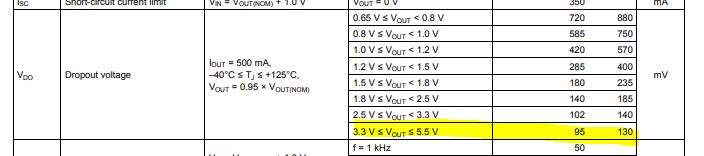
I checked our datasheet that the maximum Vdo with 500mA Iout is 115mV for this use case. But I just want to check with you if we have the Vdo data for 100mA Iout condition.

I think it should be calculated as 115mV/500mA*100mA=23mV. But I am curious that if it is just a linear relation between Vdo and Iout, why Vdo is also related to the different Vout range according to TLV758P datasheet? Thanks.

Best regards,

Wayne

  • Hi Wayne,

    While your approach is correct for many linear regulators, it is important to make sure that you are always using the current version of the datasheet.  When we released the TLV758P to marked, our maximum for dropout was increased slightly to 130 mV.

    You are correct that dropout normally has a linear relationship with Iout; however, as you can see from Figure 6 in the datasheet, dropout is closer to 40 mV at 100 mA.

    As you mentioned, there is also a relationship between Vout and dropout.  Chapter 1 of our LDO Basics e-book briefly discusses the variables that impact dropout.

    www.ti.com/.../slyy151.pdf

    For linear regulators with PMOS pass FETs, as the input/output voltages increase the minimum headroom (Vin - Vout) or dropout required for regulation will decrease.  This is because the LDO you will have a larger delta between Vin and the gate voltage which will allow the FET to be less resistive.

    www.ti.com/.../sbvy001.pdf

    Very Respectfully,

    Ryan

  • Hi Ryan,

    Thanks for your detailed explanation. It is very helpful.

    Customer has another requirement for TLV758P. They require that the output has to delay 200ms after Vin powering up. My thought is adding a RC series from Vin to GND and connect EN pin to the middle point of RC. But I am not sure about the RC value to realize a 200ms delay. What' more, the Ven(hi) is only 1V which is pretty low. So do you think this method is OK and do you have any advice on the RC value?  Thanks.

    Best regards,

    Wayne

  • Hi Wayne,

    While an RC delay on EN is a method to delay the output of an LDO, it is important to note that the enable thresholds will be between the minimum Ven(hi) and maximum Ven(lo) as shown in Figure 15.

    If precise timing is important, more robust solution is to use a voltage supervisor.  This will allow more accurate timing as output of the supervisor will provide a sharp low to high transition on EN after 200 ms after Vin crosses the desired threshold.

    Very Respectfully,

    Ryan

  • Hi Ryan,

    Thanks for your help. I have promoted TPS3808 to do the precise time delay.

    By the way, customer wants to do thermal simulation based on the software 'Flotherm XT'. So just want to check with you if we have the TLV758P simulation model for 'Flotherm XT'. Thanks.

    Best regards,

    Wayne

  • Hi Wayne,

    We do not handle these types of requests on the public forum due to the type of information we would require from the customer. I will reach out to you via Private Message to discuss further.

    Very Respectfully,
    Ryan