This thread has been locked.

If you have a related question, please click the "Ask a related question" button in the top right corner. The newly created question will be automatically linked to this question.

TPS54319: low-side MOSFET failure

Part Number: TPS54319

Hi,

we have the same issue as David Boyle1 ("TPS54319 failures"): a conducting path between PH (pins 10, 11,12) and GND (pins 3, 4). We have it on 2 out of 5 prototype boards (yet). On one board, there is a 1 ohm path from the beginning, on a second board, there has develodep a 3 ohms path after some 20 power cycles. It is very unlikely a thermal problem as we have followed the TI recommendations on thermal vias and we draw only some 0.5 amps typically (max 1 amp). The parts have the lot number C6Q7. Unfortunately, David's post has been locked. The part is powered with 5V from another TI buck converter (working fine) and outputs 3.3V to another buck converter and to a Raspberry Pi.

Can TI please tell me

- whether there is a known issue with the above-mentioned lot?

- special schematic or layout considerations necessary to avoid this issue beyond the information provided in the data sheet?

Best regards,

Christian

  • Hi Christian,
    Could you share your schematic and layout for further analysis? You can send them by email (neal-zhang@ti.com) if you don't want to post here.
  • Hi Neal,

    I have sent you the schamtic and layout via e-mail. It is a 6-layer setup with the inner layers not shown (layers 2 and 15 are GND layers and the innermost layers 3 and 14 are power and signal routing). The problem affects IC16 (yet - the 3.3V SMPS) and may also affect IC17 (the 1.8V SMPS) as it is the same part and a similar schematic and layout. We have cascaded power converters: IC9 makes 5V (+5V_RPI) out of 24V, IC16 converts 5V to 3.3V (+3V3_RPI) and IC17 converts 3.3V to 1.8V (+1V8_RPI). We have one more independant SMPS and LDO to power an MCU. We have the MCU clocking (SYNC feature) and enabling the buck converters one by one as required by the attached Raspberry Pi Compute Module and protection diodes for disabling the converters in the opposite order on sudden power loss (or another fault condition). With an unprogrammed or wrongly programmed MCU, there may be wrong enable and clock signals on unpowered TPS54319 parts. But I doubt this is actually causing this problem as all inputs are protected with resistors and the faults happen coincidentally. We have ceramic bulk capacitors with approximately the minimum recommended (well less than typical recommended due to space constraints) capacitance taking into account the DC bias derating (some 30% less than nominal value). We have added 100nF caps for fourther reducing the switching noise.

    Thank you in advance and Best regards,

    Christian

  • Christian,
    So please get your support via email and I will close this thread, thanks!
  • Hi Christian,

    I send you email but it said "your mail box rejected my message" so I posted it here

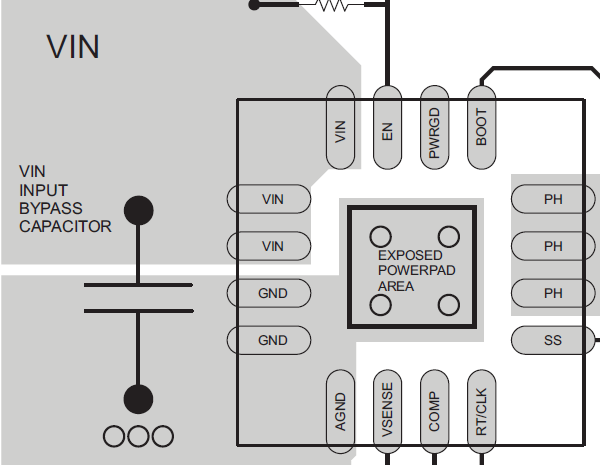
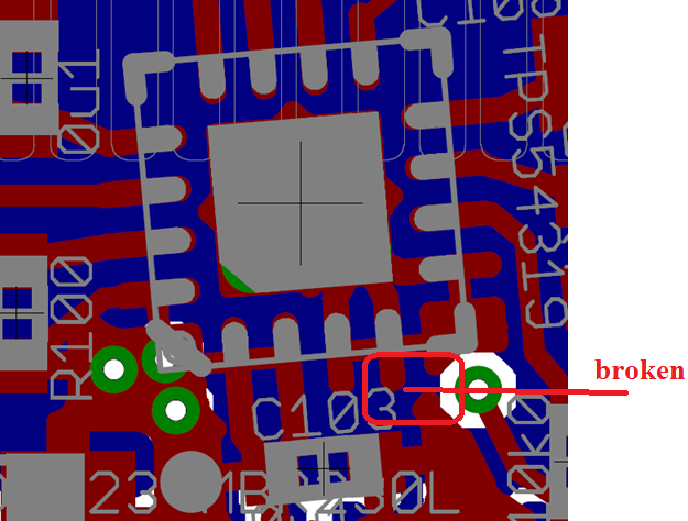
    I checked your layout and suspect the reason is caused by Vsw overshoot. For TPS54319, Cin should have very short connection to IC Vin pin(1,2) and GND PIN(3,4) . In your layout, the vin connection from c103 to IC pin1 and pin2 is two trace rather than a copper. What’s worse, the GND connection from c103 to pin3 and pin4 is broken. So there may have large parasitic inductance which result in SW overshoot. To verify that, measure the PH pin voltage, check whether it is greater than 7V (the maximum input voltage of TPS54319)