This thread has been locked.

If you have a related question, please click the "Ask a related question" button in the top right corner. The newly created question will be automatically linked to this question.

LM5141QRGEVM: Operation verification by EVM

Part Number: LM5141QRGEVM
Other Parts Discussed in Thread: LM5141-Q1

Hi,

I am an FAE of a distributor dealing with TI products.
My customer will use LM5141-Q1.
My customers will buy TI's EVM and plan to do a test before designing.
The specifications are below.
Please tell me the changes in EVM to meet the following specifications.

(specification)
VIN : 16V(min), 24V or 48V(typ), 60V(max)
VOUT : 12V
IOUT : 0.1A(typ), 3A(max)
Operating frequency : 2MHz
Operating mode : FPWM
Since the input is a battery, there are two input specifications, 24V and 48V. However, the circuit is common.
Also, the input filter is not used because the substrate size is small.
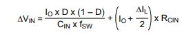
Also, I want to reduce the output capacitor as much as possible. Therefore, please tell me the minimum required capacity value.
Best regards,
  • Hello Kaji,

    please see Webench link below. You can customize desgin from here.

    webench.ti.com/.../SDP.cgi


    Hope this helps?
  • Thank you for your reply.
    At WEBENCH, I changed the input voltage to 60V.
    In that case, the input capacitor is changed to 15uF × 2 OSCON.
    Is it possible that I want to use 2.2uF x 3 in the same way as EVM?
    Also, I will not use an input filter, but does the input filter match the red circle parts in the figure below?
    Best regards,
  • One more thing I would like to ask you.
    In the WEBENCH result, the phase margin decreases when the input voltage is high and the output current is small.
    In my specification, since the TYP value of the output current is 0.1A, I want to set so that the phase margin can be secured at that time.
    How can the phase margin be increased by changing the constant of the capacitor and resistor at the COMP pin?
    Best regards,
  • Hello Kaji,

    Correct, the input filter section is as shown in the red circle above. You do not have to use the input filter, if not needed? you can use 3 x 2.2uF cermamics, just make sure if you are using long cables, that the input is well damped. This can be don't by placing a large electrolytic capacitor at the input side of your board where the Vin is connecting. Make sure its capacitance is at least 5 x 6.6uF and its ESR is alt least a few hundered milliohms.

    Hope this helps?
  • Hello Kaji,

    Please adjust to a higher value of Ccomp. say 3 x the current value. This will reduce the phase swing and ensure you have enough PM at light loads.

    Hope this helps?
  • I appreciate your advice.
    I created a circuit on WEBENCH.
    Attach the circuit you created.
    If there is a problem with the circuit, I'm glad if you give me advice.
    I think that the phase margin is enough.
    The crossover frequency is a little low because it is 12kHz, is there a problem?

    Best regards,

    WBDesign417.pdf

  • I would like to ask additional questions.
    1) In VCCENCH, CVCC = 1uF is output. 2.2uF to 4.7uF are recommended on the data sheet. Which value is appropriate for CVCC?
    2) In WEBENCH, CVDD = 1uF is output. It is 100nF or more on the data sheet, but is 1uF appropriate?
    3) At the input capacitor, I suggested to the customer 2.2uF x 3 used in EVM. However, customers want to use 0.37 uF x 1. How is the minimum value of the input capacitor calculated?
    Best regards,
  • Hello Kaji,

    In addition to my above comment, I checked the WeBench Design and it looks good to me.
  • Hello Kaji,

    The recommended Range in the datasheet is a conservative approach.  It is very unlikely that 1uF capacitor on VCC is inadequate.  if you wish to test, you can measure the ripple voltage across the CVCC and make sure the ripple does not cause a UVLO event on VCC (very unlikely).

    CVDD = 1uF is OK.

    The minimum Cin is based on two things.  

    1. The RMS ripple current rating.  This worse case IRMSCin= Iout/2.  Make sure the capacitor used is rated for Iout/2 RMS ripple current.  for a more accurate calculation, for your system refer to Equation 35 in the DS.

    2. the ripple voltage.  This becomes a fact if Vin min is close to Vout and as such the ripple voltage becomes excessive.  This usually is not an issue after point 1. above has been taken care of.

    The Delta Vin is:

    Where RCIN = ESR of CIN

    Hope this helps?