This thread has been locked.

If you have a related question, please click the "Ask a related question" button in the top right corner. The newly created question will be automatically linked to this question.

TPS62361B: Output voltage appears to follow TPS62363 behaviour

Part Number: TPS62361B
Other Parts Discussed in Thread: TPS62363, TMP103, PCA9306
We have a design where the TPS62361B is being used to generate a 0V9 digital core voltage. We’ve seen on two different samples of the same board that the voltage output is ~1.2V instead of 0.9V, which of course is not good.
VSEL0 / VSEL1 are both grounded, and the value in the SET0 register is 0x28.
With the TPS62361B, this should give 0.9V out.
With the TPS62363, the output for the same register value would be 1.17V.
Changing the SET0 register to 0x0D changes the output voltage to 0.9V, which indicates that the internal reference voltage is 770mV, not 500mV.
The Chip ID register gives 0x87, which identifies the chip as the TPS62361B, and the markings on the top of the package also supports this.
Is there anything that could make a TPS62361B behave like the TPS62363?
This is really puzzling us at the moment. Any pointers as to how this could happen would be very much appreciated.
  • Hi Jorgen,

    This does sound strange.

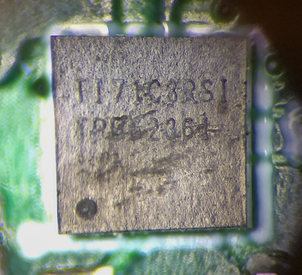
    Can you post a photo of the top of the IC, so that we can read the markings there? As well, can you post or send me (via a conversation) the label on the reel that the parts were on?

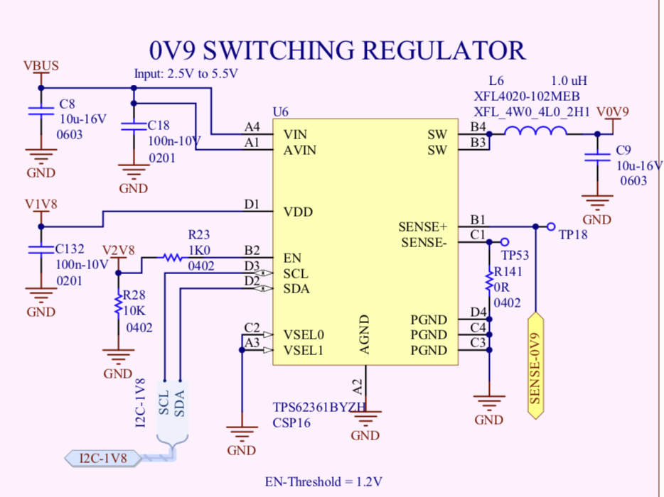
    Are VSEL0/1 hard tied to GND or are they driven with a GPIO or through a pull-up resistor? Can you post or send me your schematic around the IC?
  • Hi Chris,

    Thanks for the quick response.

    Photo of the top of the IC (a bit scratched as I had to remove a thermal pad to reveal the markings):

    Reel info, supplied from our CM:

    And, the schematics:

    As you can see, the VSEL pins are directly connected to GND.

    Best regards,

    Jørgen

  • Thanks for sharing.

    Have you used this same IC on a different board or design before? Are there other date codes which work as expected? Can you order some samples from ti.com and see if these work differently?

    Does the IC power up at 1.2V, before any I2C communication to change the voltage?

    How did you determine the SET0 and Chip ID register values? Can you double check by looking at the actual signals on the scope?

    How are the I2C pull-ups implemented?

    You are welcome to start a return with Arrow for us to double check on our side. But we can also go through these questions in parallel.
  • No problem - thanks for helping out.

    The board this is in use on is in mass production, so we've been shipping ~20K annually for a couple of years. Yield is high, and return rate is low.
    The reason it was caught on this sample was that we recently saw unusually high current consumption on a unit in our internal testing lab.
    It's probably been in use in the lab since 2017.

    I'm unsure whether the power supply has been providing 1.2V since the beginning, and that the higher than normal voltage has led to a fault developing over time in the consumer chip, or whether the power was initially providing 0.9V and has been damaged due to some sort of stress over time...

    We do not measure the voltage level in production, only unit current consumption, so we do not have statistics to show the distribution of voltage output for the MP units, unfortunately.

    But, the design has been shown to provide 0.9V with the same settings in all pre-MP samples, so we believe this is limited to some units.
    We tested yesterday on a unit produced at roughly the same time, and on this everything is OK.

    The "problematic" unit powers up with 1.2V before any I2C communication.

    We determined the SET0 and Chip ID register values through SW - carrying out an I2C read through our I2C master on the main CPU, printing to a console. I did not do a scope measurement to catch the electrical signalling. I can do this next week just to be sure.

    I2C pull-ups are quite strong - 1.5K pulled to 1V8. The following devices are on the bus:
    Master CPU - TPS62361B - TMP103 - PCA9306 level shifter to 3V3 - MMA7660 - ATSHA204A.
    Pull-ups on the 3V3 side are 2K7.

    I'll discuss with Arrow next week about a possible return.

    Thank you very much for your help - Have a good weekend!

    Jørgen
  • Thanks for explaining.

    You could also put one of the failing ICs on an EVM to see how it powers up there.
  • Hi Jorgen,

    Were you able to verify the behavior on an EVM? Did you already start a return with Arrow?
  • Hi Chris,

    We don't have an EVM available, so I haven't had the chance to move the chip over to test.
    I've started the return process with Arrow, but nothing has been shipped yet.

    Do you prefer receiving the chip on our board, or desoldered? The PCB it is on is powered from USB (USB-C connector), and is quite small. No interaction is needed with the board to start up the power supplies, so if we ship this as is, the "failure" scenario should be reproducible without any interaction except for attaching USB.

    Best regards,
    Jørgen
  • Arrow can confirm, but usually we/they want just the IC and not your board/product.

    I'll close this thread out, but feel free to reply to it if further assistance is needed.
  • Hi again Chris.

    I'm sorry to bring this issue back up, but we've completed the return and received an 8D report now that I would like to discuss with you.
    The report reference is QEM-CCR-1904-01149.

    It seems there's a bit of chipping that's occurred in one corner of the device, but I believe this could have happened when we unsoldered the chip, and that it may not be directly related to the issue we initially reported on.

    I'm more interested in figure 2 on page 4 of the report, where three pads are completely clean - no traces of solder from the solder balls after desoldering.
    Our CM commented on this and argue that this may be due to contamination or nickel penetration on the component pads before balling, leading to a mechanical connection of the balls but no inter-metallic bonding.

    I was hoping that FA would pick up on this and check solderability of these pins, but they have not tried to re-ball and functionally test the device, and instead concluded that the failure is due to the visible chipping.

    Looking at the pins that show no signs of solder flow, these are the three PGND pins on the device. I assume that the output voltage could change if there's no good connection to GND for the power output stage.

    What do you think? Is there any way we can ask for the FA team to check solderability of the device, even though they have concluded on their analysis?

    I'm worried that we have a batch related issue affecting products we have in the market. By checking the solderability, we would also be able to check if our CM's claim is true, and if not, we can also dive into whether this is due to their process / soldering profile.

    Best regards,
    Jørgen
  • Hi Jorgen,

    Our Customer Quality Engineer will contact you separately regarding your question.
    Thank you very much!

    Best Regards,
    Dorian