This thread has been locked.

If you have a related question, please click the "Ask a related question" button in the top right corner. The newly created question will be automatically linked to this question.

LM66100: OR-ing and RPP

Part Number: LM66100

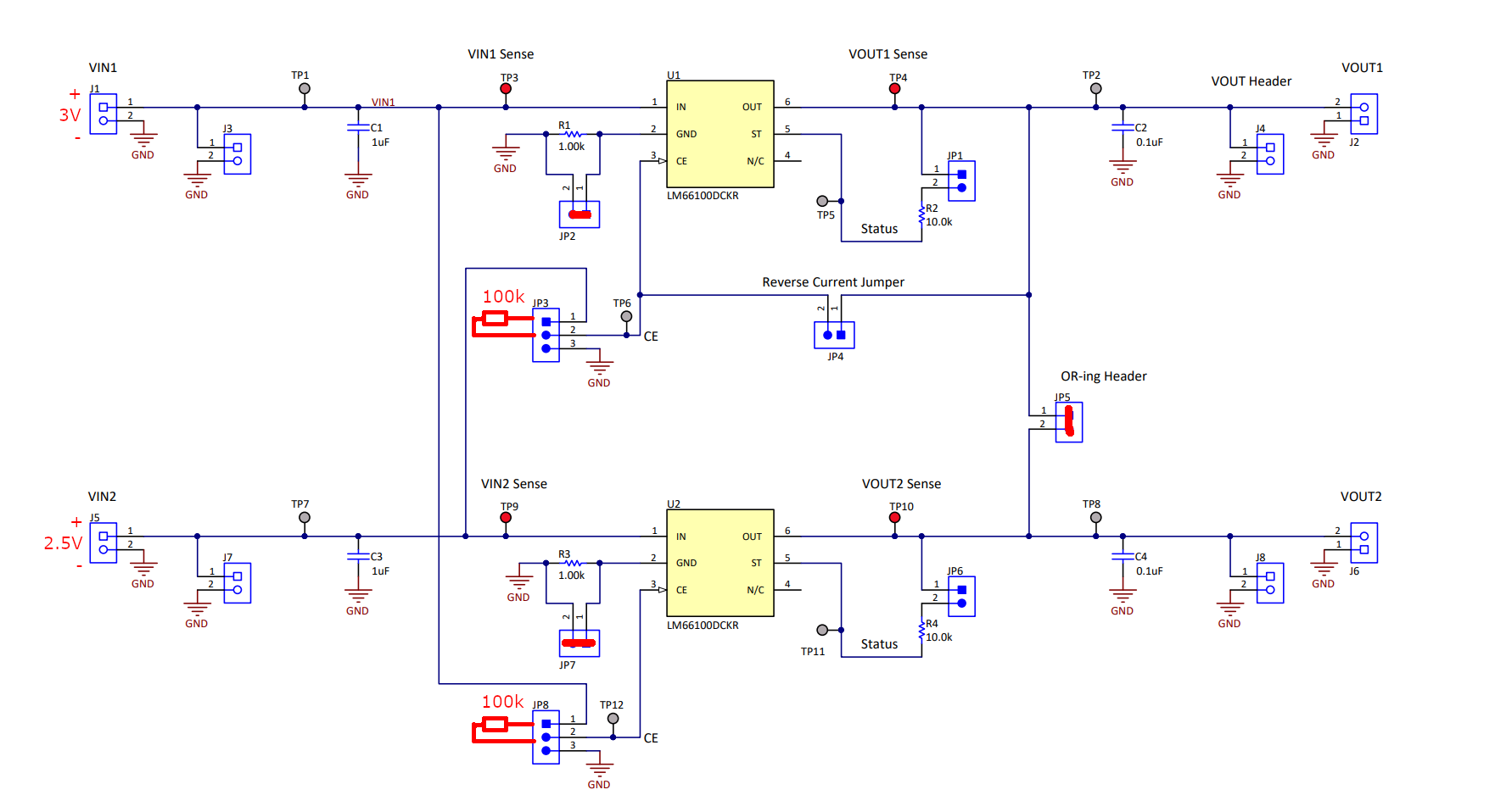
I use power ORing based on Figure 15 in SLVSEZ8A. There si one difference is 22k resistor in both CE path. ORing works well. My question is related to reverse polarity protection.

When a battery polarity is reversed, there is aprox. 123uA current flown to CE pin. This situation also do not meet declaration for CE pin -0.3 to 6V.

Is there any recomendation how to solve described situation?

  • Hi Radeg, 

    Thanks for reaching out on E2E!

    You can add a series resistor from the GND pin of the LM66100 to system GND. This will help reduce the amount of current through the CE path.

    Thanks,

    Arthur Huang

  • Hi Arthur,

    thank you for respone. Could you sugest me maximum size of serial resistance for CE pin?

    Thank you

    Radek

  • Hi Radek, 

    We don't have a maximum size for the series resistor on the CE pin. For example, on the LM666100 Evaluation board we use a 1KΩ resistor, this value could work.

    Thanks,

    Arthur

  • Dear Arthur,

    thank you for answer. I might asure you I know wery well what is written in datasheet and what is assembled on evaluation board. Im looking for information whitch is still not clear enough.

    We have worked out, that if we use serial resistance on CE pin 100k and higher, LM66100 behaves weird. I mean, switching ON/OFF is slow and do not meet expectation.

    Might I ask TI to state maximum resistance on CE pin ensuring correct behavior LM66100?

    Thank you wery much

    Radek

  • Hi Radek, 

    Can you clarify the configuration? Are you pulling up CE resistor to VIN2, or is it simply being connected to GND. If the CE pin is directly connected to GND, then the device should not be connected in an ON/OFF state. 

    Thanks,

    Arthur

  • Dear Arthur,

    please look at following scheme based on EVM. OR-ing do not work in this configuration. Approx. 3mA flows to VIN2 which is unwanted feature.

    My motivation for this configuration is to limit current when battery is reversed. But additional CE pin resistance disable ORing ability.

    1. Could you please clarify why this happen?
    2. Could you please state maximum CE pin resistance to ensure proper LMV66100 function?

    Thanks

    Radek

  • Hi Radek,

    Why do you have JP2 and JP7 shorted? We use those 1k resistors to mitigate reverse current. Do you still see this issue with those jumpers removed?

  • Hi Radek,

    Has removing JP2 and JP7 made a difference in the reverse current seen?