This thread has been locked.

If you have a related question, please click the "Ask a related question" button in the top right corner. The newly created question will be automatically linked to this question.

TLV758P: Maximum voltage rating on enable input

Part Number: TLV758P
Other Parts Discussed in Thread: TLV785, LM3880

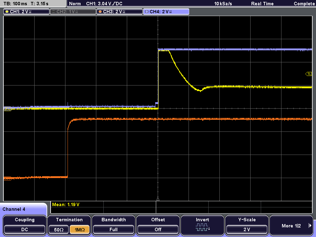
We have had a TLV75801PDRVR fail in normal operation when configured as a 1.8V regulator in a production design. The fault presents as the regulator output sawtoothing between around 1V and Vin at at about 30Hz, independent of load, but with the bulk and HF decoupling capacitors in place.

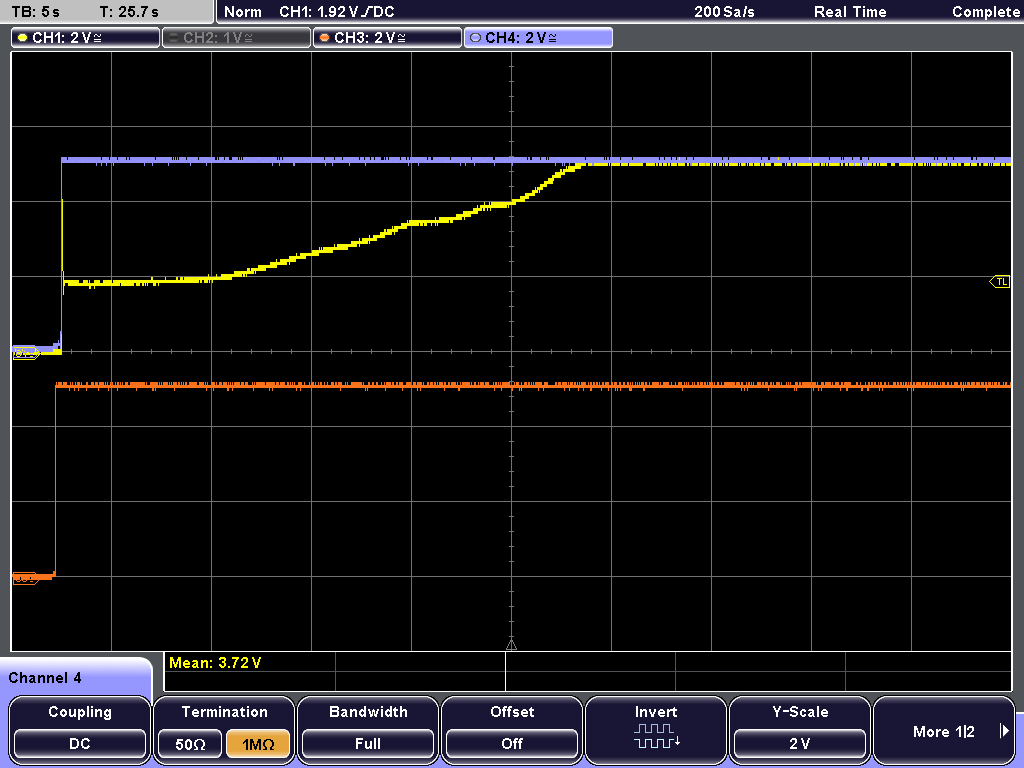
Applying a burst of freezer specifically to the TLV785 chip restores correct operation, but only while the chip is still cold. As the freezer wears off, the device starts oscillating again around its correct output, with the peak output voltage eventually climbing almost to Vin, and the amplitude of the oscillation reducing to zero around the final d.c. level.

I have been looking for possible reasons for the failure. The TLV758 data sheet gives Absolute Maximum ratings for both the Vin and En inputs of 6.5V relative to ground. It also states that Vout must not be taken more than 300mV more positive than Vin.

These conditions are unconditionally met in our design, but is there any restriction not mentioned in the data sheet on the En high voltage being greater than Vin? This condition could briefly occur in our design during unscheduled removal of input power to the board.

  • Hi Peter,

    Can you provide a scope shot of Vin, Ven, and Vout so we can see what they are all doing when this happens? My first guess is that you are running in and out of thermal shutdown given the device's reaction to the freeze spray and the very low frequency of the sawtooth. 

    You don't mention what your input voltage is or what the load is (other than to say it is independent of load), but this is a small device so the thermal dissipation is limited and it would be easy to get into thermal shutdown if the power dissipation is too high. What package variant are you using?

  • Hi Kyle,

    The suspect device is gradually changing its behaviour, so I think there is some internal damage. I have done some power-ups with the output disconnected from the load, but with the voltage divider resistors and the output capacitors in circuit (27K, 12K; 47uF // 100nF). The TLV758 sits on a thermal pad approximately 0.8 x 1.3 mm. I gave the full device part number in my initial post:: TLV75801PDRVR.

    The scope shots taken at two different timescales represent behaviour of the TLV758 from cold (a short burst of freezer).

    The bottom (red) trace is the 5V power rail that is connected to Vin on the TLV regulator, with 0V positioned on the first scope line up from the bottom of the screen. The blue trace is the En input and the yellow trace is Vout of the TLV758 configured as a 1.8V regulator. They have their 0V at the centre of the screen. All traces are 2V/div vertically.

    The first screenshot is at 100ms/div. On power-up, the TLV output goes to nearly 5V for about 30ms, then recovers to the correct 1.8V. The second screenshot shows what happens over a longer timescale (5 sec/div). The output creeps up from 1.8V to almost 5V over a period of about 30 seconds. Application of a further squirt of freezer brings the output back to 1.8V, and causes the drifting high behaviour to repeat The sawtooth oscillation behaviour I orginally reported has disappeared.

    The regulator supplies the 1.8V rail of a medium-size Xilinx Spartan 7 FPGA, but is only required to deliver about 50mA. I could relatively easily replace the suspect TLV758, but the FPGA ,and as a consequence the whole complex board is is part of, is now unusable except for the sort of tests I am carrying out. The 1.0V and 3.3V rails of the FPGA are also regulated via TLV758s supplied from the 5V rail. These two are as yet still working correctly.

    Peter

  • Hey Peter,

    Can you try re-attaching the screenshots? they didn't come through. 

  • Very odd. I purposely checked on a completely separate computer that my post was fully visible on the TI forum. Anyway, I'll include the two screenshots again in this post, and if you report that you can't see these either, I'll devise a different method. For information, I used the "Insert/Edit Media" button in the toolbar.

  • Hi Peter,

    Thank you for reposting the scope shots they worked this time and along with your description it is very informative and clearly rules out thermal shutdown.  

    As to your question if there is any requirement that Ven<Vin, the answer is no the device will not be directly damaged if Ven is greater than Vin the two can operate independently. That being said, we recently found that if VEN > VUVLO rising (min), the input supply must be capable of sinking 1 mA of current to avoid the device being turn on with a floating input pin (we are working to update the PDS to state this) but this seems unlikely to damage the LDO.  

    Looking at the behavior shown in the scope shots it looks as if there may be some leakage current from FB to GND. This can happen either because of board contamination or a damaged LDO. Given that you're seeing it consistently change vs temperature I'd lean more towards damage on the LDO FB pin since board level leakage is unlikely to change very significantly with freeze spray. Do you have a feedforward cap installed (Cff goes form Vout to FB)? If so very large transients on the output could couple through Cff to the FB node and cause the voltage to exceed an Abs Max voltage on FB. 

    Another common cause would be an ESD event which damaged the device.  

  • Hi Kyle,

    Thanks for your comments. There is no feedback capacitor on any of the three TLV758 parts generating the power rails into the FPGA.

    I have done a little more investigation on the damaged board. I have shown (1) the En input of the TLV758 still can switch the output on and off, even if the output is at its runaway level, and (2) the FB input of the TLV758 does follow the output voltage in the expected ratio during the misbehaviour, and the voltage at the FB pin is rising well above its datasheet value. I have checked the GND pin on the TLV758, and it remains firmly at 0V.

    The FB pin observation reduces the likelihood that board-level effects could be changing the effective resistor ratio from Vout to FB, with the FB input remaining at a constant voltage.Additionally, using carefully applied freezer spray, the temperature infuence on the fault behaviour is very specific to the TLV758, and does not appear to be related to surrounding components or board surface properties.

    In our design, the sequence for powering up and down for the three rails is managed by an LM3880, which sequences in the order 1V0, 1V8, 3V3 on power up and the reverse on power down (if the supply 5V rail lasts long enough - depends on other loads). There is an MC34161 voltage monitor that holds off the individual enables of the TLVs if previous rails in the sequence have not managed to rise close to their required voltage. The monitoring was primarily for preventing FPGA damage through mis-sequencing if there was a board fault that caused a failure of a rail to get to its prescribed level.

    The 1V8 and the 1V0 rails feed the FPGA core, and are purely loads. Under certain fault conditions, the 3V3 rail has the possibility of being reverse powered from the FPGA via other logic connections if the 3V3 TLV758 is held off, but this rail has shown no sign of a problem. The over-voltage fault is with the 1V8 rail, the middle one of the sequence.

    These TLV parts are located in the centre of the board with no direct connection to the I/O on the outside. Even the 5V supply rail is generated by an on-board isolated dc-dc converter. The board is fully enclosed in a metal chassis. The engineer who was using the unit told me it had been running normally for at least half an hour before it began to show problems. On observing a problem, he stopped the run he was on and cycled the mains power to the unit. The problems got worse, and he brought it to me for investigation. I observed the 1V8 rail to the FPGA had a sawtooth waveform on it, as I originally reported. Further running reduced the waveforms to those I have captured and reproduced here.

    As far as I can see, there was no possibility of an external damaging influence on the TLV758 that failed. Its failure has resulted in an expensive board being written off. My concern is whether this was an unfortunate one-off component failure, or whether it could indicate a design weakness in the TLV758 part. We need to be confident that the TLV758 is a reliable device that can safely be used for powering relatively costly FPGAs, preferably without the need for narrow window voltage monitoring of its outputs.

  • Hi Peter,

    I understand your concerns, my team works very had to validate all of our new LDOs very rigorously before new designs are released in order to try and eliminate the chances of customer's having issues like yours. We put our new designs through tens of thousands of transients to try and catch anything that might hint at a potential design flaw (plus the usual industry standard reliability testing). It's not impossible that we might miss something but it seems unlikely that we'd miss something like this which seems to have a pretty normal startup sequence.  

    The fact that the FB node is tracking Vout (and the reference) indicates that the output is being pulled up by some sort of leakage and isn't being regulated by the error amplifier to an incorrect voltage. So if there isn't any other leakage path from the 5V rail to the 1.8V, then the most likely source of that leakage is from Vin to Vout through the LDO's pass device. There is always a small amount of leakage through the pass device but a damaged pass device can leak significantly more, and that leakage will increase exponentially as the temperature increases (which correlates with your cold spray test). 

    You mentioned that you are powering an FPGA, and while the power up /down sequencing is always such that you don't see any reverse current, one common situation we come across is that some loads need to be programmed/flashed and the input voltages to the regulators powering the load must be powered down while so the programming can happen. This can cause reverse current damage, can you confirm if there is the possibility of any such event during the manufacturing/testing process? 

    As for the possibility of an ESD event, when we see this sort of damage it often comes up during the manufacturing process since most designs do not have the LDOs connected to the outside world in any way. 

  • Hi Kyle,

    I've been away for a couple of days and have just got back to this.

    The FPGAs we use are volatile and need to be loaded from an external memory on each power-up. In this design, we use an I2C EEPROM memory, programmed during production (or on update in the field) though logic levels at normal rail voltages. There is no flash programming or any other process that uses elevated voltages.

    The scope photos that I posted of the board's output voltage behaviour were taken with the voltage regulator disconnected from the FPGA. There is no significant change to the behaviour pattern if the regulator powers the FPGA.

    I'm not convinced that the regulator's error amplifier loses control of the output in the fault state, since the enable input works as expected, retaining the ability to switch the output from 100mV below Vin to ground and back again as a square-edged waveform.

    I noted a further significant point during use of the freezer spray to produce a temperature cycle. If I held Ven low for about 20 seconds after the freezer squirt, the output is kept off, but releasing Ven sends the output to the false overvoltage level that it would have reached had the enable remained high, To me, this doesn't feel like it's necessarily the pass device that has the problem.

    The Functional Block Diagram (paragraph 7.2 in the data sheet) shows the enable input controlling the band-gap reference. The error amplifier presumably compares the FB voltage against the BG output voltage to generate the gate potential for the pass device. Could the problem be the BG reference output going wild, rather than pass device damage or leakage? This could explain why I see the voltage at the FB input staying the correct fraction of the output voltage at all times, fault condition or no fault condition.

  • Hey Peter,

    You mentioned that "In this design, we use an I2C EEPROM memory, programmed during production (or on update in the field) though logic levels at normal rail voltages. There is no flash programming or any other process that uses elevated voltages." but are any of these programming signals applied to the LDO's output while the LDO's input is at a lower value? The voltages don't have to be "elevated" to damage the LDO, they would only need to be 300mV above Vin to exceed the Abs Max voltage of the output pin listed in the datasheet. 

    It does seem like if you can disable the part then the pass device may not be the source of the issue. As for your question "Could the problem be the BG reference output going wild, rather than pass device damage or leakage?" It is a possible explanation of the behavior but the likelihood seems low unless it was damaged somehow, but nothing in your application that I've seen hints at a way to damage the BG reference. Every device is tested before being shipped and an incorrect BG reference would fail testing. 

  • Hi Kyle,

    I was somewhat simplifying the other sections of the design in my description. The FPGA loading on power-up is done by an STM32 CPU with the FPGA as an I/O peripheral. The CPU is held in reset until the FPGA power rails are sequenced up. The CPU takes the FPGA image data from the Quad SPI flash EEPROM and loads it into the FPGA using 3.3V I/O. 

    Initial configuration writing of the EEPROM (production phase) and any subsequent writing (field updating) is purely a function of the CPU and the EEPROM; the FPGA is not involved. Not until the next power cycle does the FPGA receive the new image through the CPU.

    The regulators for the FPGA rails and the separate ones for the CPU and EEPROM section are supplied by a common 5V line. Everything is quiescent until that 5V line is present and supplying the Vin pins of all the local regulators, so there can be no activity on the FPGA LDO outputs without 5V on their inputs. In addition, the only LDO that could be affected by external voltages is the one supplying the 3V3 I/O rails, and that's not the one showing the output problem.

    I fully accept that all your devices have to pass stringent test procedures, and it's one of the reasons that we have been using TI (and BB) parts for over 50 years. It's unlikely that this particular TLV758 failure would have been picked up in your production testing, as it worked without trouble in our board for over 3 months before the problem manifested itself. The other TLV758s in that particular board and the ones in all the other pre-production boards have, so far, not shown any sign of this problem. We may just have to accept this was a one-off failure, but that we should consider going back to incorporating window comparators rather than just level comparators on all our critical voltage rails.

  • Re-posting this as it did not seem to have got to the Forum.

    Hi Kyle,

    I was somewhat simplifying the other sections of the design in my description. The FPGA loading on power-up is done by an STM32 CPU with the FPGA as an I/O peripheral. The CPU is held in reset until the FPGA power rails are sequenced up. The CPU takes the FPGA image data from the Quad SPI flash EEPROM and loads it into the FPGA using 3.3V I/O. 

    Initial configuration writing of the EEPROM (production phase) and any subsequent writing (field updating) is purely a function of the CPU and the EEPROM; the FPGA is not involved. Not until the next power cycle does the FPGA receive the new image through the CPU.

    The regulators for the FPGA rails and the separate ones for the CPU and EEPROM section are supplied by a common 5V line. Everything is quiescent until that 5V line is present and supplying the Vin pins of all the local regulators, so there can be no activity on the FPGA LDO outputs without 5V on their inputs. In addition, the only LDO that could be affected by external voltages is the one supplying the 3V3 I/O rails, and that's not the one showing the output problem.

    I fully accept that all your devices have to pass stringent test procedures, and it's one of the reasons that we have been using TI (and BB) parts for over 50 years. It's unlikely that this particular TLV758 failure would have been picked up in your production testing, as it worked without trouble in our board for over 3 months before the problem manifested itself. The other TLV758s in that particular board and the ones in all the other pre-production boards have, so far, not shown any sign of this problem. We may just have to accept this was a one-off failure, but that we should consider going back to incorporating window comparators rather than just level comparators on all our critical voltage rails.

    Peter

  • Hi Peter,

    Thank you for the additional detail, it explains the use case well and I agree that the programming sequence shouldn't be exposing the devices to reverse current since the 5V input is present. 

    As you indicated, this seems to be a one-off failure.