Hi team,
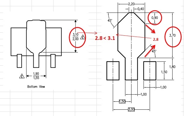
Could you help me explain why package and footprint of dimension are different? Is correct?
This thread has been locked.
If you have a related question, please click the "Ask a related question" button in the top right corner. The newly created question will be automatically linked to this question.
Hi team,
Could you help me explain why package and footprint of dimension are different? Is correct?
Jimmy,
I agree this is confusing, I'm not sure which package info is correct, let me ask our design team and get back to you this week with this info.
Thanks,
Abhinav.
Hi Jimmy,
This is correct. The first image is the dimensions of the package. The 2nd image is the land pattern. A land pattern is always bigger to accommodate the solder flow and have space for the solder to make contact with the board. If the land pattern was the same size as the package then there is no way to hand solder the device.
The names highlighted in purple are probably just due to different revisions. This does not affect the validity of the information . Other packages have similar discrepancies in the name.
Do you have any more concerns?
-Marcoo
Hi Marco,
Sorry about my description let you confusing, I knew the land pattern must bigger than dimensions of the package.
My customer's concern that a land pattern of shaping compare with the package are different
In other words, land pattern top side looks like trapezoid but package top side looks like a rectangle.
Another vender's package and land pattern of shaping are both same.
refer as below.
Actually, customer another concern as below.
somewhere land pattern small than the package. Is the result right?

Hi Jimmy,
I understand the concern. The 0.9 section was added because the longer part is only 2.8. So with the total of 3.7, there will be room for the solder. Every vendor has a different footprint. As long as the footprint follows IPC-7351 they should all be valid.
The engineering reason is on note D. trapezoidal walls will allow for better paste release.
-Marcoo