This thread has been locked.
If you have a related question, please click the "Ask a related question" button in the top right corner. The newly created question will be automatically linked to this question.
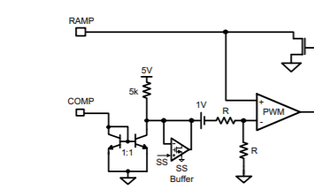
My customer is modeling this pin as part of their MATLAB control loop simulation. Do you know what the transfer function is?
We know it is not a linear one between 0mA to 1mA because we can put as much as 500uA into the COMP pin without moving the duty cycle away from maximum (COMP pin open).
Please advise. Thank you!
You can calculate the relationship between the duty cycle and COMP value by regarding the PWM section of the block schematic
in the LM5045 data sheet.
V_ = (Vcomp-1)/2
Vcomp = 5(1-Icomp)
This gives V_ = 2- 2.5*Icomp
The minimum value of RAMP signal is zero since the LM5045 has a blanking function at the start of each clock cycle.
The value of Icomp corresponding to maximum duty cycle occurs when V_ = V+ =0.
This state corresponds to Icomp = 2/2.5 = 0.8mA
Now you need to know the peak value of the RAMP used in your application.
This is normally set at 1.5V
When V_ = 1.5V the duty cycle is minimum
This state corresponds to Icomp =( 2-1.5)/2.5 = 0.2mA
Between 0.2mA and 0.8mA the PWM varies linearly.
You can use the block schematic above to generate the transfer function.
Regards
John
Regards
John
John, I really appreciate the detailed and rapid response!
There is one thing I'm not tracking on though. You are saying maximum duty cycle occurs at the maximum current and minimum duty cycle at a lower current. But this is opposite of what the data sheet says and what we see in practice. Specifically, the data sheet says that leaving COMP open (zero current) runs the PWM open loop at maximum duty cycle (50% nom) while 1mA of COMP input current forces minimum duty cycle (0%). This is consistent with what we see on the bench and also consistent with what an opto-coupler output driven by a shunt regulator input would provide.
What am I misunderstanding?