


Other Parts Discussed in Thread: TPSM846C23
Hi,
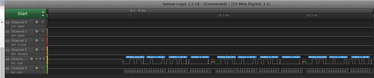
I am trying to establish IC2 communication between TPSM846C23EVM-806 and TIVA TM4C1294XL to control the output voltage of the TPSM846C23EVM whose default voltage is 0.6V. I would like to set it to 0.35 V. Here is the part of my code for that. The code works fine as you can see the snapshot of the logic analyzer below. My question is that it does not work without the time delay (SysCtlDelay(50)) that I included after every data byte transition. It took a while from me to figure out that I need to include a certain delay but I do not know the main reason? I was thinking that checking the BUSY bit should be enough but apparently it is not. Could you please let me know the reason for the need of a certain delay after every data byte transmission. Thanks a lot...
Note: The second snapshot of the logic analyzer shows the results after removing the time delay.
int
main(void)
{
uint32_t ui32SysClkFreq;
uint8_t VOUT_COMMAND[3];
ui32SysClkFreq = SysCtlClockFreqSet((SYSCTL_XTAL_25MHZ | SYSCTL_OSC_MAIN | SYSCTL_USE_PLL | SYSCTL_CFG_VCO_480), 120000000);
SysCtlPeripheralEnable(SYSCTL_PERIPH_GPIOG);
//
// Wait for the Peripheral to be ready for programming
//
while(!SysCtlPeripheralReady(SYSCTL_PERIPH_GPIOG));
//
// Stop the Clock, Reset and Enable I2C Module
// in Master Function
//
SysCtlPeripheralDisable(SYSCTL_PERIPH_I2C1);
SysCtlPeripheralReset(SYSCTL_PERIPH_I2C1);
SysCtlPeripheralEnable(SYSCTL_PERIPH_I2C1);
//
// Config pin muxing for I2C and select I2C function for these pin
//
GPIOPinConfigure(GPIO_PG1_I2C1SDA);
GPIOPinTypeI2C(GPIO_PORTG_BASE, GPIO_PIN_1);
GPIOPinConfigure(GPIO_PG0_I2C1SCL);
GPIOPinTypeI2CSCL(GPIO_PORTG_BASE, GPIO_PIN_0);
//
// Wait for the Peripheral to be ready for programming
//
while(!SysCtlPeripheralReady(SYSCTL_PERIPH_I2C1));
I2CMasterInitExpClk(I2C1_BASE, ui32SysClkFreq, true); // The rate of the clk for I2C1 module is set to 400 Kbps.
I2CTxFIFOFlush(I2C1_BASE); // Flush the transmit (TX) FIFO.
VOUT_COMMAND[0] = 0x21; // register to be written.
VOUT_COMMAND[1] = 0xB4; // LSB
VOUT_COMMAND[2] = 0x00; // MSB -- sets the output voltage to (0x00B4) 180 * 2^-9 = ~ 0.35 V.
while (1)
{
I2CMasterSlaveAddrSet(I2C1_BASE, TPSM846C23_I2C_ADRESSS, false); // I2C1 Master is initiating a write to the slave at address of TPSM846C23_I2C_ADRESSS.
I2CMasterDataPut(I2C1_BASE, VOUT_COMMAND[0]); // Place the data (register address) to be sent in the data register
I2CMasterControl(I2C1_BASE, I2C_MASTER_CMD_BURST_SEND_START); // Initiate send of data from Master to Slave
SysCtlDelay(50);
while(I2CMasterBusy(I2C1_BASE)); // Delay until transmission completes
I2CMasterDataPut(I2C1_BASE, VOUT_COMMAND[1]); // Place the data (MSB) to be sent in the data register
I2CMasterControl(I2C1_BASE, I2C_MASTER_CMD_BURST_SEND_CONT); // Initiate send of data from Master to Slave
SysCtlDelay(50);
while(I2CMasterBusy(I2C1_BASE)); // Delay until transmission completes
I2CMasterDataPut(I2C1_BASE, VOUT_COMMAND[2]); // Place the data (MSB) to be sent in the data register
I2CMasterControl(I2C1_BASE, I2C_MASTER_CMD_BURST_SEND_FINISH); // Initiate send of data from Master to Slave
SysCtlDelay(50);
while(I2CMasterBusy(I2C1_BASE)); // Delay until transmission completes
}
}
FIRST SNAPSHOT (WITH TIME DELAY)
SECOND SNAPSHOT (WITHOUT TIME DELAY)


