This thread has been locked.

If you have a related question, please click the "Ask a related question" button in the top right corner. The newly created question will be automatically linked to this question.

TPS7A37: Instability issues on output or bad soldering?

Part Number: TPS7A37
Other Parts Discussed in Thread: LP5912, LP5907, TPS63710, , TPS7A87

Hi everyone,

I have designed a multi-stage PS that outputs

1) +5.0V (LP5912)

2) +5.0V (LP5912)

3) +3.3V (LP5907)

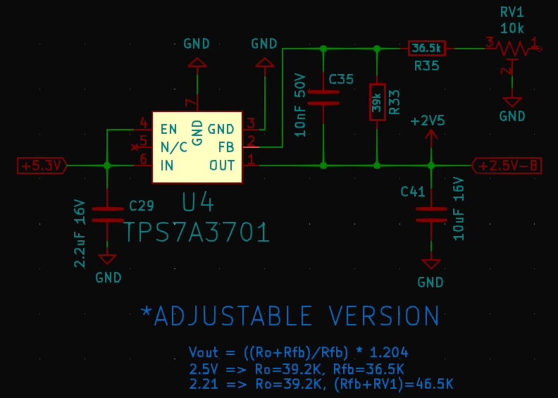
4) +2.2-2.5V (TPS7A3701 - Adjustable version)

5) -2.2-2.5V (TPS63710 & ADP7183)

I have lot's of experience on pcb design and during the last 3-4 years in 6-layer implementations.

The current implementation is a 6-layer:

  1. (Top layer) GND + small signals
  2. GND+ power signals mostly
  3. GND+ power signals mostly
  4. GND + 5.3V plane (under TPS7A3701) + power signals mostly
  5. GND
  6. (Bottom layer) GND

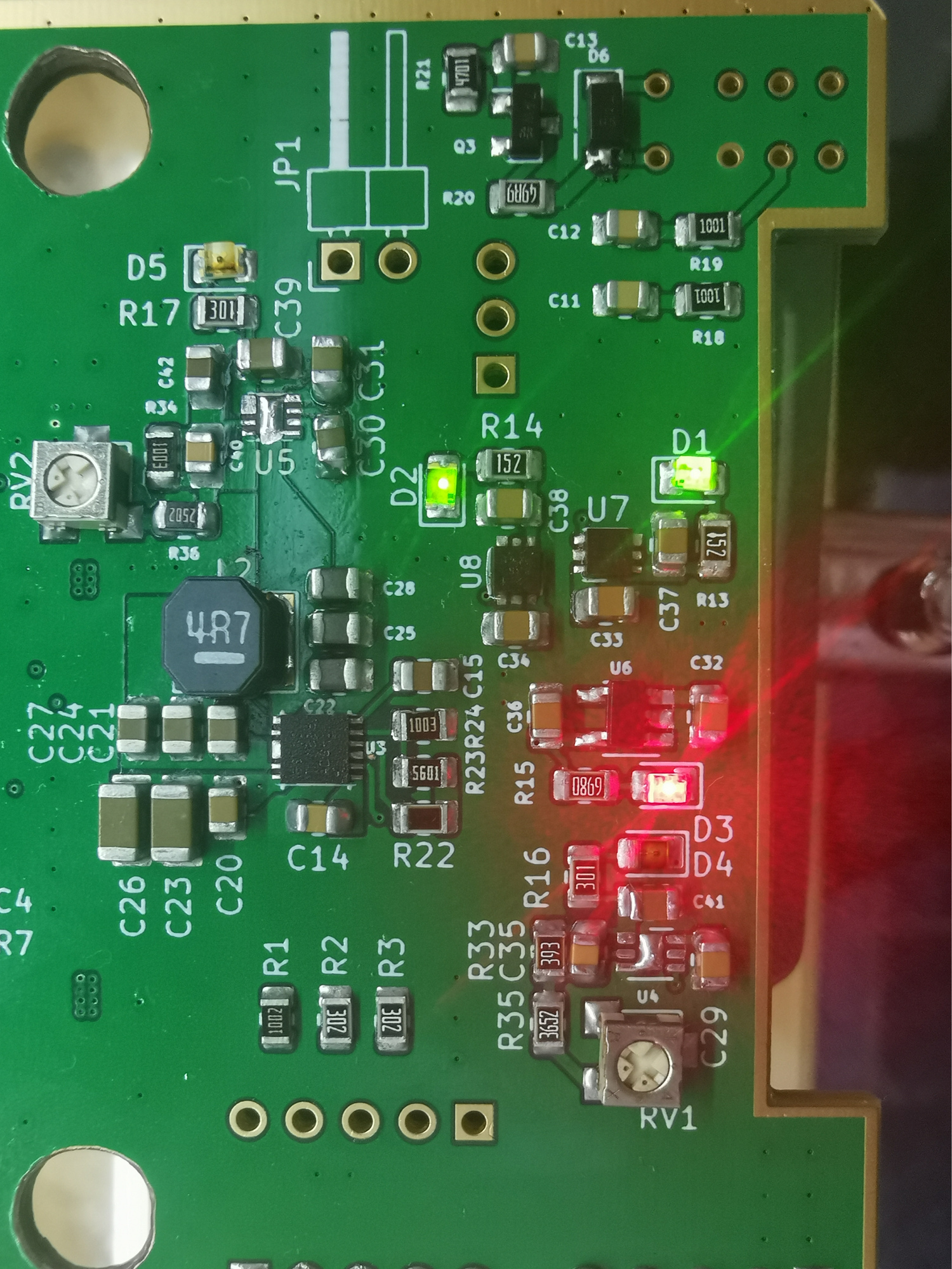
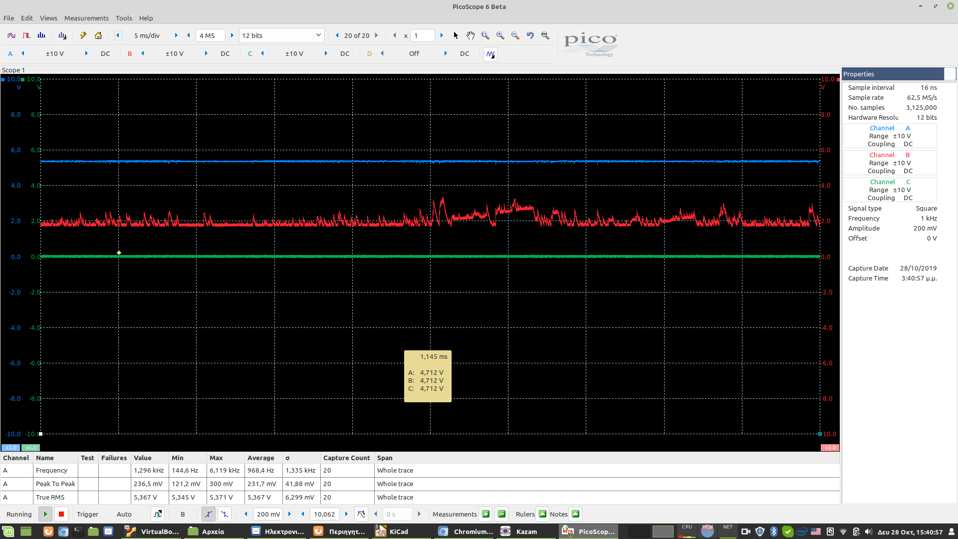
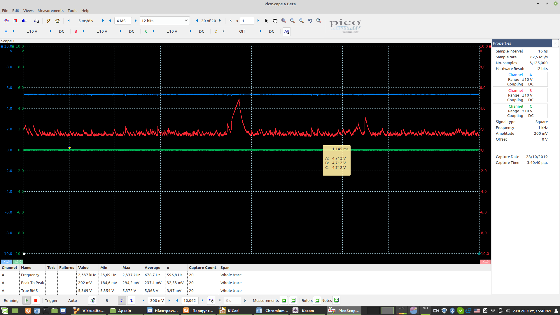
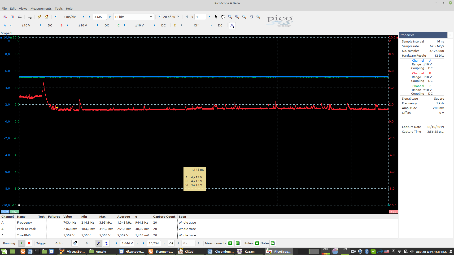
I have leds on all outputs with the correct R in series so that i can see whether any of the outputs are having issues (at least those that can affect the led illumination).

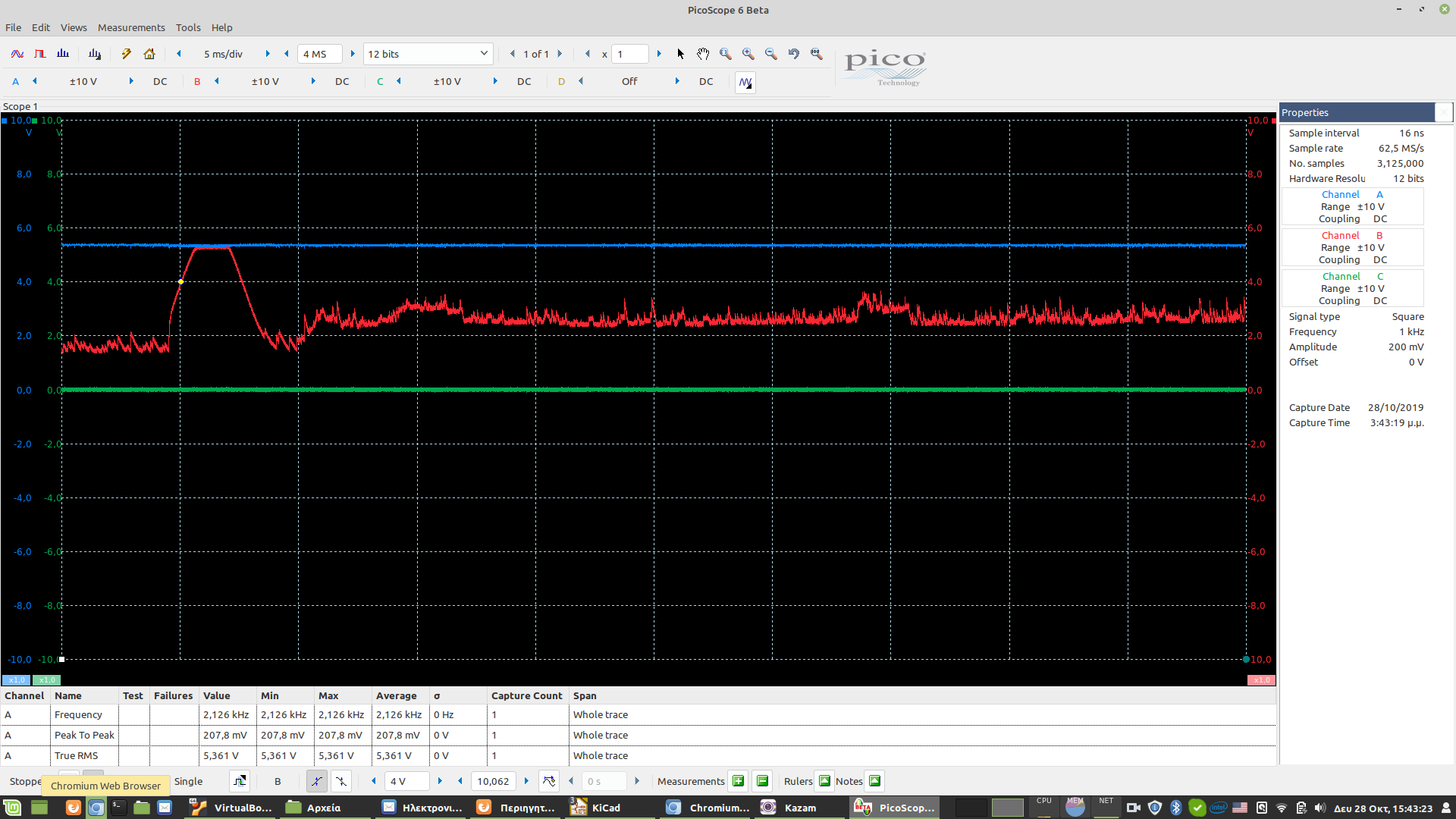
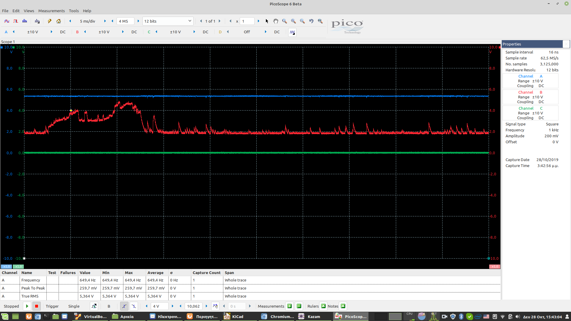
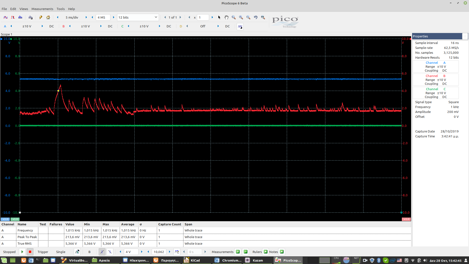
The 5.0V outputs work fine and so does the 3.3V. The TPS63710 output also works exceptionally well with my DMM reading -3.00V every single time i measured.

All measurements were done with no load except for one of the +5.0V outputs where a two Atmel microcontroller stage is connected.

I am feeding all PS stages inputs with 5.3V from my bench PS except for the ADP7183 which is supplied by the the TPS63710 with -3.0V.

The TPS7A3701 & ADP7183 are making my life soooo hard.

*I do not expect any comments regarding ADP7183. I am just mentioning the fact which could help you jump into usefull conclusions.

TPS7A3701:

I used solder paste + hot airgun during my first attempt. The led did not light up. I unsoldered and re-soldered the same part (2nd attempt) using lots of flux. Visibly, i can tell you that everything looked perfect. I used a microscope to see if the soldering was good and everything seemed fine. Moments later the led started lighting up but not in a stable way. It was more or less trembling (going on & off very fast). I went on with a 3rd attempt with a NEW part. The led lighted up and the voltage adjustment range was pretty close to the one mentioned above +2.2-2.5V. I think that it was about 15 mins later when the led looked brighter and when i measured the output, it was 5.3V (same with the input). I re-did an unsoldering and re-soldering of the same part (attempt 4) and the result was about the same. I then used the hotair gun over the chip @ 100 deg celcius for 30sec or so and it worked fine for maybe half an hour until i quit (for today).

ADP7183:

I do not remember exactly how it behaved but i can tell you that it was not stable. Some times trembling, sometimes it stayed off for long then went on for a bit longer and so on. The second attempt on the 2nd part gave me a more stable result with the stability being good for maybe an hour. Then it went off then trembling and so on.

I am really confused. I do not know what on earth i did wrong. I do not know why the problem persists on the two -/+2.5V outputs. I do not know why the others are fine and the two -/+2.5V are making my life hard.

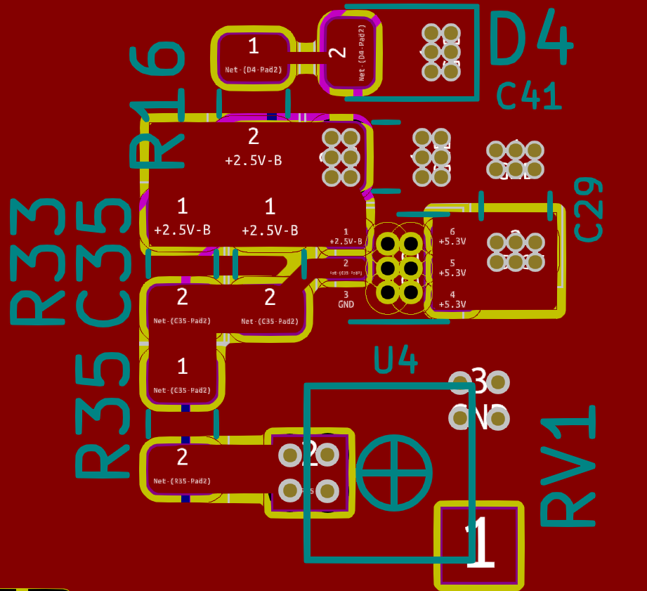
I know that the layout plays a key role in the stability, the input & output caps, the quality of the caps (X7R or even better COG). I used X7R at 16V which is much higher than the working voltage (as biasing reduces capacitance) rails and capacity higher than the one required to ensure stability.

Did i over-do it with the 10uF at the output of the TPS7A3701?

Is it the stress from the high temp air gun? ( i have done it 1000 times on other smd ICs)

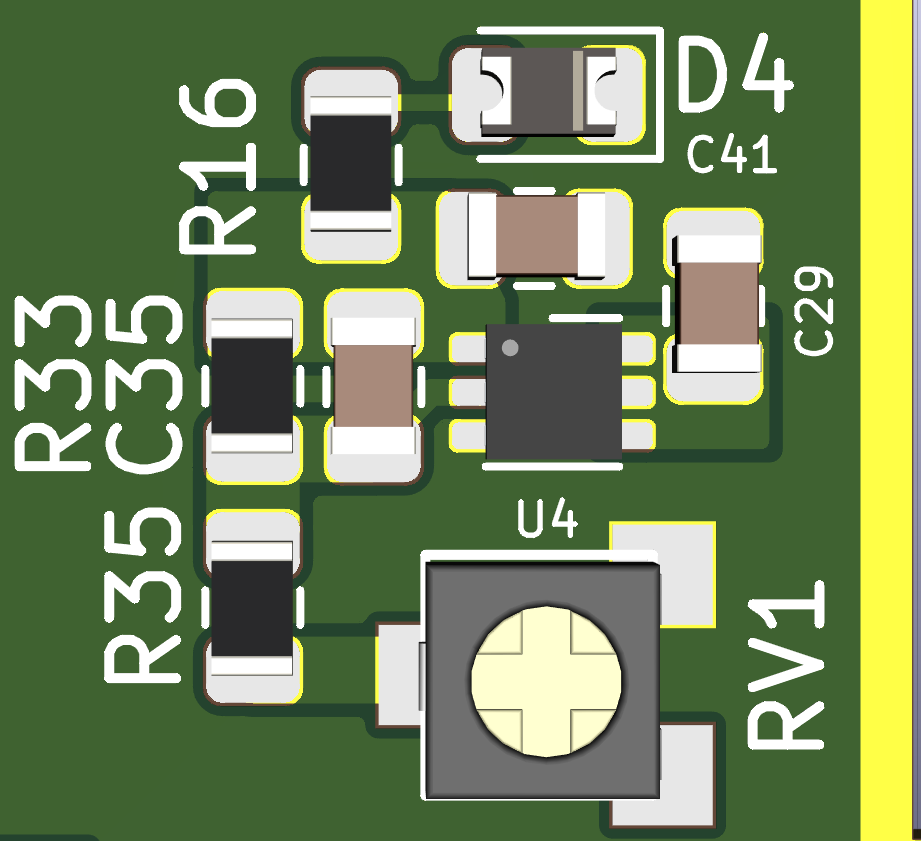
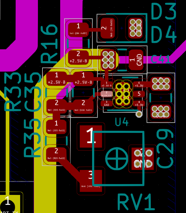
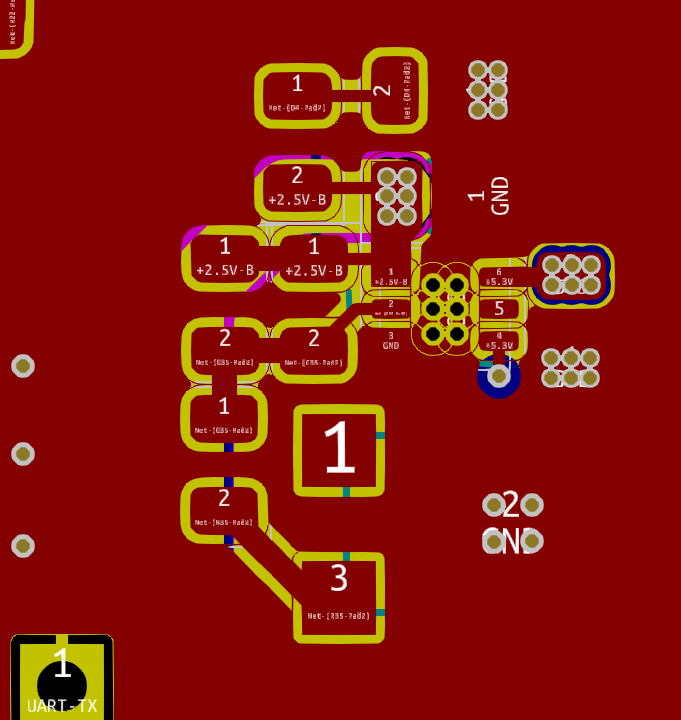
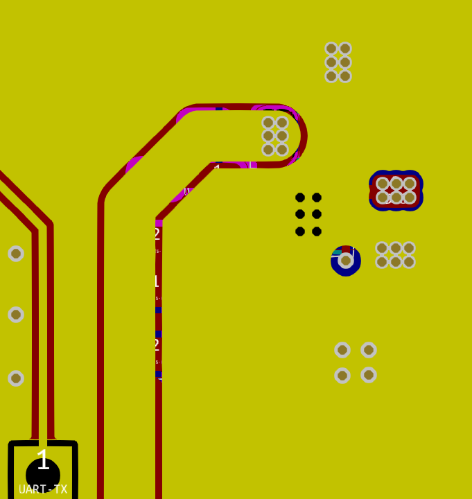
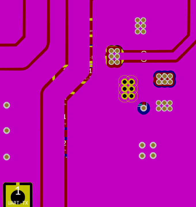
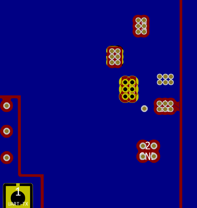
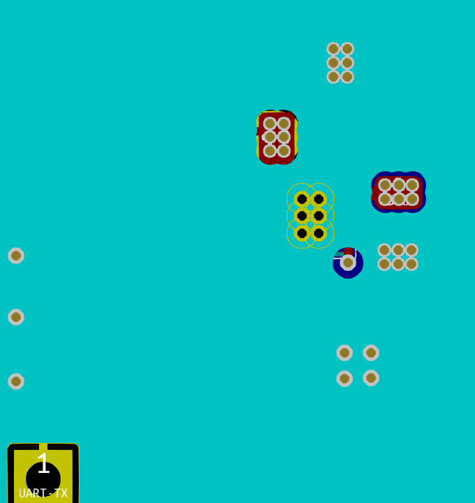
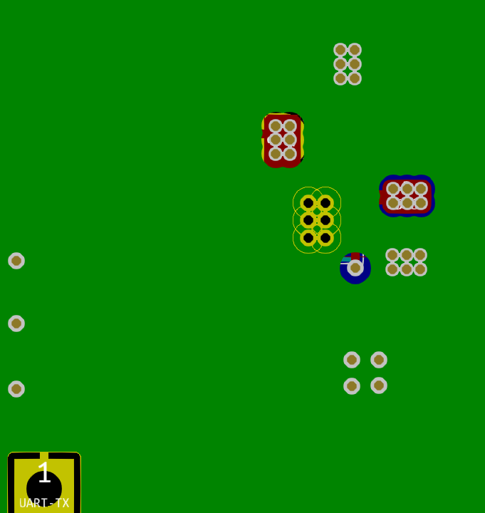
Is it the layout? I know that the decoupling caps must be really close to the in/out pins. Please see below

Is it some weird phenomenon that i am missing here?

Is it that the 5.3V is too close to the upper 5.5V input rail limit?

Is it just that the soldering has to be just perfect?

Is it the tiny dust particles between the pins?

Do you see anything wrong in the schematic?

Is it the input trace that is too thin? Just noticed it...

Is it the aliens?

The TPS7A3701 is a humidity level 2 sensitivity device and came from mouser.com inside a bag with the related card with the coloured round sections which were the correct colour at the time i opened the bags but also during the subsequent soldering of the second part. So i did not bake the device.

TOP LAYER + SILK SCREEN ^

TOP LAYER  ^

INNER LAYER 1 ^

INNER LAYER 2 ^

INNER LAYER 3 ^

INNER LAYER 4 ^

BOTTOM LAYER ^

I could use any help that you can give me right now. I have been working on my project for months (not just this PS) and this is really stressing.

Best Regards

Emmanouil Tsachalidis

  • Hi Emmanouil,

    I will be happy to assist.  We will work together to try and troubleshoot the issues with the TPS7A37.
    I am off site but when I return to the office on Monday, I will check some of my notes regarding this device.
    I will be unable to assist with the ADP7183 due to it being an Analog Devices component, and we simply do not have background information on this linear regulator including any abnormalities which it might display.
    I can look into a TI drop in replacement, if one exists, in case you find there is an inherent flaw in the ADP7183.

    Let's start with the basics.
    1. Your output capacitor of 10uF is well within the datasheet requirements.
    2. Your selection of feedback resistors is well within the datasheet requirements
    3. Your schematic looks fine for the TPS7A37.
    4. Given the amount of work you have already done, I do not suspect dust particles is the problem.

    What we need to do is some basic troubleshooting.
    Q: Do we know if the inputs to the linear regulator match the outputs?
    A: If you have an oscilloscope, please measure the Vin, EN and Vout pins.  During the state when the LED was blinking, do we see power to the LDO browning out?  Do we see the EN pin browning out?  Is there unusual behavior with the input signals and do they exceed the max ratings of the part?

    Q: Are there more than 1 ground in the system?
    A: Confirm that the grounds are shorted, and nothing is accidentally "floating". I have seen many failures in the past with floating grounds, so lets get that out of the way immediately.  Also confirm that the input grounds are connected to the source supply ground.

    Q: Does the LED flashing match the Vout of the LDO?
    A: This test is confirming the issue is around the LDO, and not the LED.  If you have another board you can test with, measure the impedance between the LDO and LED and confirm it is a short.  Then if you see the LED blinking, check the direct output of the LDO and confirm it is also "blinking".

    Q: Do we know if there is an inherent short in the PCB that ties the output to the input?
    A: If you have a bare board PCB, can you make a multimeter measurement between the input and output to confirm high impedance?

    Q: Are we hitting a protection feature?
    A: What is the load current of the LDO?  Is it high or low current?  Are there large transient peaks on the output that could cause the LDO to enter a over current protection or thermal protection?  What kind of device is the LDO powering?

    Q: Is there noise in the system coupling into the LDO causing it to misbehave?
    A: We will wait on this, but a quick test would be to remove the Cff capacitor as it is not needed for stability.  If there were conducted EMI going back into the LDO, the Cff capacitor would look like an AC short and could cause some transients to enter the LDO, be magnified by the error amplifier, and disrupt the setpoint voltage.  This phenomenon is not specific to a TI LDO, it can be any LDO by any manufacturer.  This phenomenon is uncommon but can happen.

    Q: On the inner layer 1, is the thin yellow trace the 2.5V output power path?  What is the rest of the yellow copper?  GND or Vin?

    Thanks,

    - Stephen

  • EDITTED:

    Hi Stephen,

    Here is my comments in red:

    What we need to do is some basic troubleshooting.
    Q: Do we know if the inputs to the linear regulator match the outputs?
    A: If you have an oscilloscope, please measure the Vin, EN and Vout pins.  During the state when the LED was blinking, do we see power to the LDO browning out?  Do we see the EN pin browning out?  Is there unusual behavior with the input signals and do they exceed the max ratings of the part?

    EN pins are connected directy to the Vin which is the 5.3V rail. See at the bottom of the post.

    Q: Are there more than 1 ground in the system?
    A: Confirm that the grounds are shorted, and nothing is accidentally "floating". I have seen many failures in the past with floating grounds, so lets get that out of the way immediately.  Also confirm that the input grounds are connected to the source supply ground.

    All layers are mostly GND connected with the rest of the other layers with lots of vias. So there is no chance that any of the GNDs in the other layers are floating.

    Q: Does the LED flashing match the Vout of the LDO?
    A: This test is confirming the issue is around the LDO, and not the LED.  If you have another board you can test with, measure the impedance between the LDO and LED and confirm it is a short.  Then if you see the LED blinking, check the direct output of the LDO and confirm it is also "blinking".

    That was measured with a DMM but yes there is a sync between the led illumination & the output voltage. It can be easily seen in the DSO screenshots.

    Q: Do we know if there is an inherent short in the PCB that ties the output to the input?
    A: If you have a bare board PCB, can you make a multimeter measurement between the input and output to confirm high impedance?

    There was a 300K and rising slowly. I observed up to 500K. It was still increasing... *That was measured with the TPS NOT soldered on the pcb.

    Q: Are we hitting a protection feature?
    A: What is the load current of the LDO?  Is it high or low current?  Are there large transient peaks on the output that could cause the LDO to enter a over current protection or thermal protection?  What kind of device is the LDO powering?

    The total input current being drawn by the PS stages on the pcb is read on the bench PS lcd that i have built maybe 10 years ago (based on a mega32) and is around 30mA. That alone can be a guaranty that we are not having any high output currents anywhere in the PS stages due to short circuits or other abnormalities. That was my guide most of the time when i soldered the TPS7A37 & the ADP7183. 30mA is a normal current being drawn by the microcontrollers connected to one of the (LP5912) +5.0V supplies. There were moments where this indication increased up to 70-80mA or was going up and down. It was then that i noticed the leds blinking.

    Q: Is there noise in the system coupling into the LDO causing it to misbehave?
    A: We will wait on this, but a quick test would be to remove the Cff capacitor as it is not needed for stability.  If there were conducted EMI going back into the LDO, the Cff capacitor would look like an AC short and could cause some transients to enter the LDO, be magnified by the error amplifier, and disrupt the setpoint voltage.  This phenomenon is not specific to a TI LDO, it can be any LDO by any manufacturer.  This phenomenon is uncommon but can happen.

    I did unsolder the CFF between the TPS output and the FB pin. I saw no difference in the behavior.

    Q: On the inner layer 1, is the thin yellow trace the 2.5V output power path?  What is the rest of the yellow copper?  GND or Vin?

    That is the +2.5V connecting the TPS7A37 output to a pin header. The rest is GND.


    This is a top view of the PS stages ^ with the TPS7A37 & ADP7183 being unsoldered


    What follows is a set of screenshots taken from my dso. Honestly with the soldering & unsoldering that taken place i am not sure whether the part in question is after all a non-damaged part.


    These ^ are screen shots from the Vin (Blue) vs Vo (Red). Green was supposed to be the EN but i have measured a zero impedance with the +5.3V.


    I did one screen shot ^ with the GREEN DSO probe connected to the EN pin because it was really close to the MLCC cap next to it and it was really difficult to do it without short circuiting the +5.3V with the GND.

    Please let me know what you think...

    Regards

    Manos Tsachalidis

  • Hi Stephen,

    The conclusion that all this mess is taking me to is that i have to solder the TPS in just the perfect position.

    For crying out loud, this is a 6-pin linear regulator, not a BGA 1000 pin IC!

    I will try my last part tomorrow morning after removing as much solder from the pads as possible and applying just the perfect amount of solder paste.

    Wish me luck...

    Regards

    Manos

  • Hello Manos,

    I am still reviewing your latest data and comments.
    I would like to have another reply back to you tonight or tomorrow morning.

    I wanted to let you know that I reviewed the archives on the TPS7A3701, and nothing of significance came up that is not already in the datasheet related to your questions.  I also asked a colleague about a drop in replacement for the Analog Devices LDO, in case you discover an issue with it and choose to make a change.  The TPS7A87 is our closest replacement without considering further requirements that you may have.

    Thanks,

    - Stephen

  • Hello Manos,

    These are very interesting oscilloscope plots.
    The Vin (EN) waveform looks solid.

    If you have time for anything: try changing the output cap to something lower, like 2.2uF or 1uF.
    If the component is not hitting a protection limit of some kind, and it is not being affected by noise, it could be a stability issue.
    Lowering the output capacitor may make a difference for this component.

    You are following the proper guidance for placement of ceramic capacitors near the board edge.
    Still, it is worth noting that the LDO which is experiencing the issue is with the capacitor near the board edge.
    Could cracked ceramic capacitors be the root cause?  Have you replaced the capacitors recently?
    If you have not, it may be worth a shot, as replacing the LDO's could have placed enough heat on the ceramic cap to damage it.
    Be very careful and try not to heat up the capacitor too much during the replacement effort.
    Ceramic capacitors are known for being brittle and can become cracked due to board flexures and thermal shock (solder iron applied directly to the capacitor pad).  The idea is to apply the solder iron tip to the PCB pad, and let the solder reflow to the ceramic capacitor as quickly as practically possible.

    Do you know if anything could be pulling transients at about 1-10KHz rate? 
    Some of those pulses on Vout look to be in that frequency range.

    Do you have any way of measuring the current with a current probe to detect current transients?

    A last resort could be to remove the LDO, wire in an external bench supply at low current limit settings, and carefully turn up the voltage. 
    If the external bench supply went into current limit then you would know that something in the system is pulling additional current beyond our expectations.
    You can accomplish something similar by using an IR camera, if one is available, to look for any unexpected hot spots on the CCA which would indicate abnormal behavior or a short circuit. 

    I'll look for your response and reply back with additional feedback.

    Thanks,

    - Stephen

  • Hi Stephen and thanks so much for the support,

    I did what i said i will, that is, i replaced the TPS using my last part.

    Before powering up, i removed both Vin & Vo MLCC caps. I did a really good cleaning with alccohol and cotton buds looking for bad solder joints or anything visibly abnormal.

    I couldn't find anything so i supplier the PS stages with the 5.3V rail. Everything looked fine with the trimmer adjustment range being 2.22-2.49V which is just perfect.

    Maybe 5 mins later, the led started trembling or flickering or whatever you want to call it.

    I removed the trimmer and bridged the two pads that the trimmer was using to apply the adjustment range. I now had constant 2.49-2.50V.

    Moments later, the flickering started again.

    It was clearly visible that the led was going brighter at times, then completely off then wandering around the 2.5V level and so on...

    I then unsoldered the resistors forming the feedback network, then cleaned again thoroughly and then re-soldered the old feedback resistors and the old Vin & Vo caps.

    I powered up again, with the trimmer unsoldered, and i saw that the 2.5V was steady at 2.5V. I then re-soldered the trimmer and adjusted it all the way to confirm the range did not change in any way and so it was. The range was fine starting at 2.22V up to 2.49V which is the required range.

    I then connected a 6.8Ohm resistive load at the 2.5V output. I could measure 2.48V with the load connected and 2.49V without load.

    My bench PS was showing around 37mA without the 6.8Ohm resistor connected and around 403mA with the resistive load connected.

    I left the load connected for maybe a hour (and will leave it much longer) with the output being steady as never before.

    The bench PS is configured to shut down the output if over current conditions are detected instead of limiting the output voltage. In this way i know for sure that no current limiting occurs. That was intentionally set up like this to avoid confusion.

    I really do not know what to think... This is what is killing me the most, a tiny fragment of uncertainty which does not guaranty that if i connect the load to the 2.5V it will stay at 2.5V and won't go to 5.3V because if it does that then lot's of opamp circuits will be damaged.

    I am thinking about improving the pcb design a bit.

    - The pins 4, 5 & 6 should be tied up together thus giving the chance to increase the width (not length) of the Vin trace in order to minimise parasitic inductance.

    - Add a few vias right at the GND pad of the decoupling caps. I have debating the placing of vias on the pads of smds but i have seen that, although solder is being sucked a bit in the vias, it frees up space for other components and makes GND returning paths impedance lower (at least DC paths).

    I haven't got a current probe that can measure so low currents and certainly not a IR camera. Thermal performance, as i noticed, was quite good with the 6.8Ohm resistor connected. I could touch the TPS with my lower lip and feel the heat. The heat however was not that high for me to remove my lip after let's say 5 or 10 secs. I could hold it there for quite longer. That has to be less than 40 deg celcius which is excelent. My target output current at 2.5V is around 250mA which is less than the one i am testing!

    So i will leave it like this for a day or so, i mean with the 6.8Ohm resistor connected. If it starts going nuts again, chances are the output will reach the 5.3V rail. If that happens, the overcurrent protection of the bench PS will be triggered and i will then know.

    Your comments regarding cracked caps or components damaged by excessive heat are true. I just took my chances by using the same components after measuring their value with no abnormalities being found there but there is always a chance that you could be right.

    I am trying to assemble a prototype of the project i am working on and this mess has driven me nuts.

    Regards

    Manos

  • Hi Stephen,

    Too good to be true... Although i am sure that the TPS part is intact, there has to be something else wrong.

    After working flawlessly for an hour or so, it suddenly started going up and down again...

    Waiting for your last comments before i make changes to the pcb and send it over for manufacturing.

    I am out of time really...

    *I had a look at the evaluation board with the fixed voltage TPS7A37. I did not notice anything that could help me.

    Regards

    Manos

  • Hi Stephen,

    I will give it a shot later today by playing with the output cap.

    I measured a lot of spikes at the output of the bench PS. After having a look to the DS i saw that ringing due to a input transient is a possibility and is output-cap-ESR dependent. So i will see if i have any other cap & ESR values that can fit in there.

    Manos

  • Hi Stephen,

    I have made some improvements to the pcb.

    I am using the pin 5 (N/C) in order to minimize 5.3V impedance path from the Vin cap to the Vin pin.

    I have also brought the GNDs of the Vin & Vo caps together to form a star topology (if you can call it that).

    I also added vias to the GND pads of the Vin & Vo caps (no vias before) to form direct paths to the other layers.

    I have also increased the width of the traces of the feedback loop but that is not that important because no significant currents flow through them, but instead i mostly did it for mechanical strength against soldering.

    Please have a look and compare with the old pcb in my prev posts:

    Regards

    Manos

  • Hi Stephen,

    I reversed the Vin & Vo caps and it seems to "work". I mean that i soldered the 10μF at the input to compensate for the input high transients coming from the bench PS and the 2.2μF was soldered at the output.

    The trimmer was adjusted so that the output is @ 2.30V. It's been 30mins and it still seems ok.

    I will come back with more info when available.

    Regards

    Manos

  • Nop, same mess...

    After some time the output started going to the 5.3V at random times.

    Now it is stuck at 5.3V.

    I do not know what to think anymore...

    Manos

  • Hi Stephen,

    Unfortunately i am again at where i started.

    The dam thing is just not gonna work.

    An hour later, the problems restarted...

    I am going to a redesign.

    Please let me know if you have anything else to add or i will close the thread.

    Thanks again for your time

    Manos