Hi, Jaden
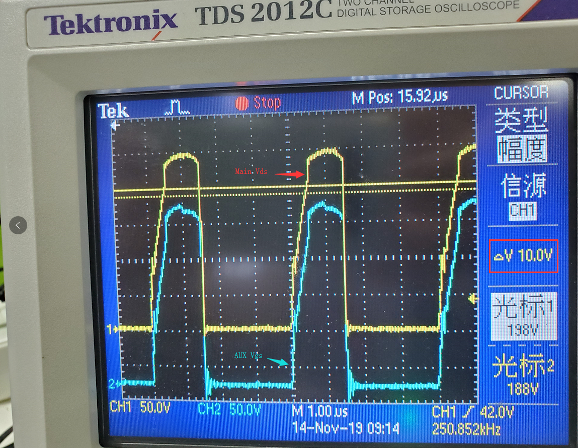
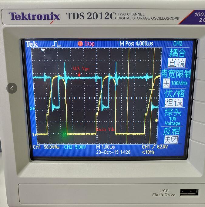
Please look at my waveform and see if ZVS has been implemented. And I feel the rising edge of the main switch Vds is a little strange, do not know what is the reason, according to the principle should be vertical up.

Original question:

Hi, Jaden
Please look at my waveform and see if ZVS has been implemented. And I feel the rising edge of the main switch Vds is a little strange, do not know what is the reason, according to the principle should be vertical up.