This thread has been locked.

If you have a related question, please click the "Ask a related question" button in the top right corner. The newly created question will be automatically linked to this question.

TPS22994: TPS22994 "not working" as expected

Part Number: TPS22994
Other Parts Discussed in Thread: TPS22917, TPS22924

Hi,

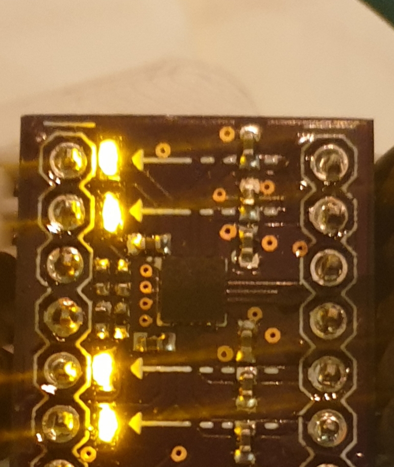
I created my own breakout for TPS22994 a while back and wrote a simply library for it.
In an evaulation for a IOT device I'm using quite a powerhungry wireless module drawing way too much current in sleep mode.
The wireless device is known to have spikes up to 2amp (few ms) and then staying in the range of 30-60 during active mode.

Since I'm breadboarding I needed a way to control power-on to the wireless module so I placed my TPS22994 breakout board.
Placed my LiPO single cell on the inputs of all of them (4) by bridging them together. Connected all four outputs to the wireless module.
Then run the SwitchALL command. The 2amp spikes are known to come after a few seconds. On the wireless module there is a 100uF oversized cap.
Though it would be ample time to get that charge to handle the spikes by its-self.

The wireless module behaves badly and wont work when behind the TPS22994. If I act as the switch by connecting the wireless module manually to the lipo instead of the TPS22994  it works as expected.
The TPS22994 should handle 1amp per channel but I guess there is something in the details I'm missing.

Off course I wont use the TPS22994 in my design but opt for a single channel load switch like TPS27081A or maybe smaller formfactor TPS22916.

But I would really like to understand whats happening here. 
I think it could be related to my Slewrate or Quick Output Discharge (QOD) Control settings.

  • .....staying in the range of 30-60 mA during active mode

  • Hi Fredrik,

    Most of the folks are out due to holidays. We will get back by early next week.

    BR, Rakesh

  • I added control of on-delay, slew-rate and qod to my library.

    So at boot-up of my mcu I configure channel 1-4 (address 01h-04h) with a 0 setting which should meen highest slew rate and no on-delay and so on.

    Still same issue. I dont have an scope where i'm currently sitting but realize that would be the way to start of this troubleshooting. Any one here who could theorize a bit on what's not working?

    Would really appreciate that!
    ... When people are back from their holidays off course!! :-) 

    A note on capacitors from the datasheet... "For the fastest slew rate setting of the device, a CIN to CL ratio of at least 100 to 1 is recommended to minimize VIN dip caused by inrush currents during startup"

    My breakout only has 1uF on both Cin and CL... Unfortunately I went for a 0402 footprint so limited in what I can add in terms of increasing Cin...
    But I could add them in via breadboard ...

  • Added a common CIN for all outputs and common CL for all inputs. Tried values ranging from 10uF to 100uF. Tried ratio 100:1 and 10:1.
    Did not help...

    I added some code to check that my register settings are correct.
    The default 14 yields 
     

         ON  SLEW QOD
    x | 0 0 | 0 1 1 | 0 0   = 14

    Slew = 011 = 460 µs/V   

    ------ Output from test-run --------------------------


    Check Register Conf default values
    Channel 1 conf=14
    Channel 2 conf=14
    Channel 3 conf=14
    Channel 4 conf=14

    Setting On-Delay, Slewrate & QOD to Agressive mode

    Check Register Conf values
    Channel 1 conf=0
    Channel 2 conf=0
    Channel 3 conf=0
    Channel 4 conf=0

    Enabling all channels via SwitchALL with slewrate = 1 µs/V


    All channels are turned on...

    Input and Output channel trace widths are 0.6mm. Online PCB trace widths calculators states 0.3mm should be enough on outer layers for 1amp of current for 1-inch traces.
    Using 0.7mm finished vias for output channel 2 and 3. Tried to folllow layout guide best I could. 

  •  The initial question was really about my usecase of the TPS22994 by bridging inputs and the outputs getting effectively a single channel handling around 2 amps. Looking at the lastest release (2014 :-)) of the datasheets actually has this usecase added to it. Not sure why I stumbled across the first release.

    Never mind the problem is not solved.

    Looked into the capacitor on the input of the wireless module.... It's not 100uF ... Its actually 1000uF.

    SMD Capacitor 6.3V Tantalum Capacitor 1000uf 6.3V 108j 6L3R1 E-Type to be more precise.

    Not really sure what is going on here. I'm tuning on power via TPS22994 at least 1 sec prior to the wireless module tries to connect to tower (where the 2amp spikes are seen). So what could be wrong here... 

    Looked at a lot load swtich videos to understand te use case and  I think this fits nicely. Is there something in the datasheet for this particular ic I'm missing??
    Sounds like using a load switch aims at taking a lot of the problems away for the designer. 

    The only scope I can resort to is my nearby bitscope. Not sure that is up for the task...


  • Ok. So I started measuring the voltage on the input capacitor (1000uF) of the wireless module. 

    Battery is at 4.0 voltage (fully charged 1500mAh)
    Power on the module connected directly to the battery  and it drops to 3.2 V...
    Placed it behind the TPS22994 ... It's a 2.6 V... So the voltage drop is to big...

    So back to CIN vs CL ratio which is kind of off.

    Cin of 10uF and I'm thinking that that large cap on wireless bat pin servers as a CL so.... Losts of capacitance on output...
    Maybe remove the 1000uF and replace with something more appropriate..

    Datasheet of the actual module states 330uF when a placed beind a DC-DC.

    Also "Ensure that the input voltage never drops below 3.0V even when current consumption rises to 2A in the transmit burst. If the power voltage drops below 3.0V, the module may be shut down automatically"

    Removed the load and still measure 0.5V drop over input/output....


  • Oooops... Started looking at Ron and got back to max specs...

    Input Voltage: 1.0 V to 3.6 V 

    Time maybe to look at that new load switch I thought I needed in the first place...

    TPS22917  

    • Input Operating Voltage Range (VIN): 1 V–5.5 V
    • Maximum Continuous Current (IMAX): 2 A

    So would B version fit my usecase?

  • While doing another breakout with the TPS22917 I went through my drawers... Had a breakout for a single package that integrates a P and N−Channel MOSFET  (On's NTJD1155L). 1.5-8V. 1.3amp sustained with shorts peak close to 4 amp.

    This worked right off the bat (no pun intended).
     

    So. This is more than likely lack of understanding on my part but not really sure where the ease of use comes in using the TPS22994. Thinking there must be something with my PCB layout that creates the drop.. I didn't do for any capacitors in the solution above...

  • Hi Fredrik,

    Apologies for the slower response times, most of us were out these past few days.

    It looks like you have managed to work through your issue on your end.

    Just to give you a few overarching statements, the Cin to Cout ratio is a guideline more to protect supplies than to protect the device. During large inrush spikes, the input could droop low enough for the device turn on to be affected. This is not a hard recommendation if the supply is strong.

    I see that TPS22917 seems to work better for you. You stated "B version"; to what are you referring? 

  • Hi,

    No have not tried the TPS22917 yet. In the process of ordering a breakout pcb. But the ON chip does work.
    So stil not sure why the voltage drop is that big and hard to overcome using my current settings.

    Any pointers?

  • Hi Fredrik,

    If you are still committed to using the TPS22924 for this use case, I would recommend taking a few scope shots that describe the issue when the lights do not turn on.

    I would like to see input voltage, output voltage, EN and output current if possible.