This thread has been locked.

If you have a related question, please click the "Ask a related question" button in the top right corner. The newly created question will be automatically linked to this question.

ISO5451-Q1: Noise issue on top gate signal

Part Number: ISO5451-Q1
Other Parts Discussed in Thread: ISO5451, TMS320F280049, ISO5851

I have the following:

  • 4 switch 3-phase interleaved bi-directional buck boost converter (please refer to TMS320F280049: CMPSS query to implement peak current mode control of a 4 switch 3-phase interleaved bi-directional buck boost converter post for a diagram of my setup)
  • 2 boards in total: Controller Board and Power Board
  • 12 gate signals
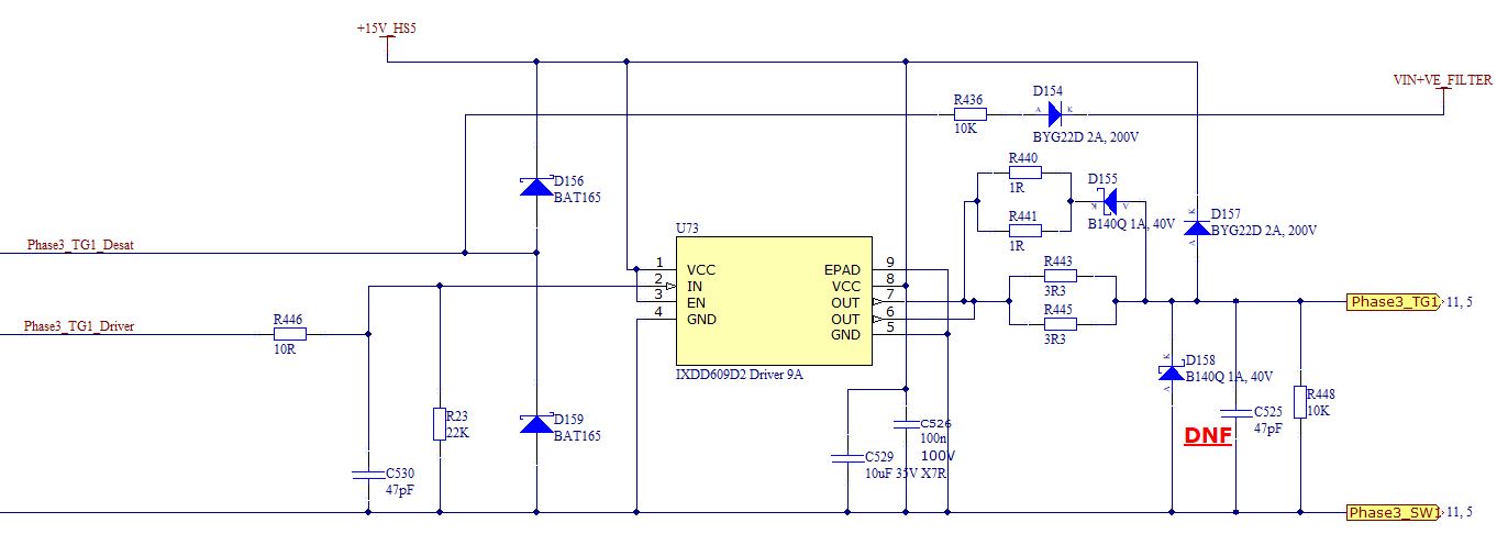
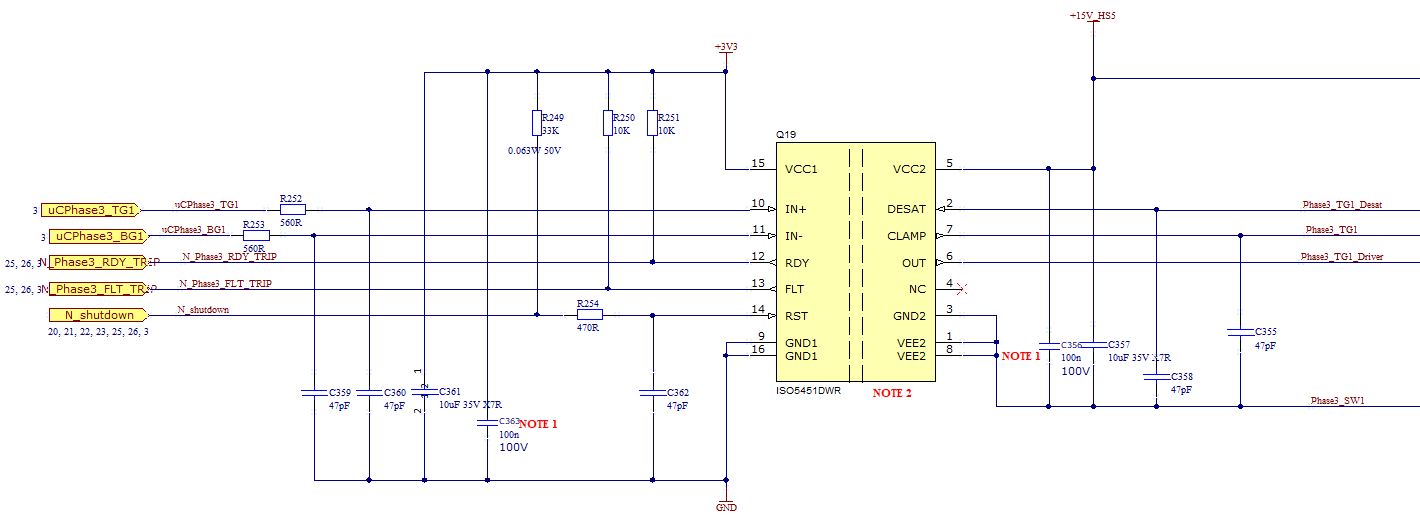
  • 12 ISO5451 gate drivers are on the Controller Board
  • 12 IXYS IXDD609 buffers on the Power Board
  • All 12 gate driver circuits are schematically identical
  • The gate signal connections are connected via non-ideal long track traces from the Controller Board to the Power Board
  • The switching frequency is 70kHz
  • All gate signals to the ISO5451 are generated using the PWM module of the TMS320F280049
  • The TMS320F280049 is operating at a 100MHz clock frequency
  • The tests were done with no inductor present and no supply voltage across the bridge
  • Desat protection and miller clamp is part of the circuit and permanently enabled
  • 22nF gate capacitance of each MOSFET
  • 0 to 15V gate signals

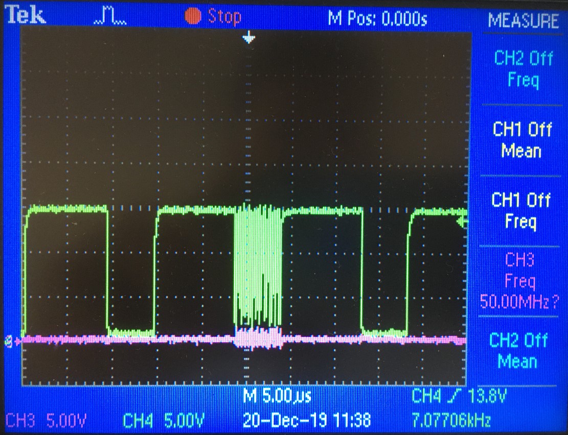
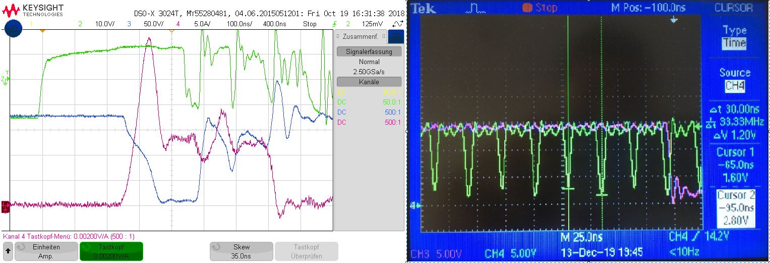
Out of the 12 gate drivers, I have a problem with one displaying the following characteristics causing a shoot-through.

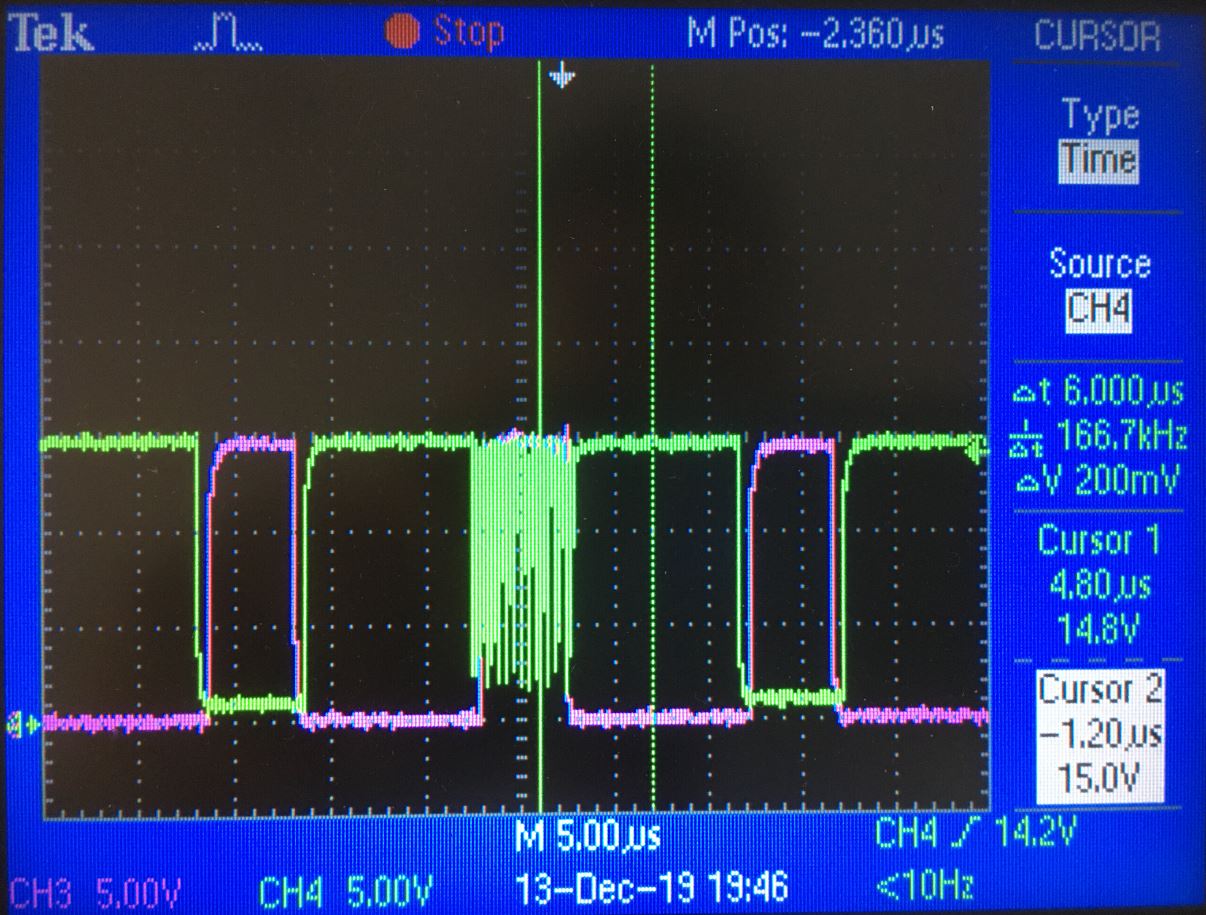
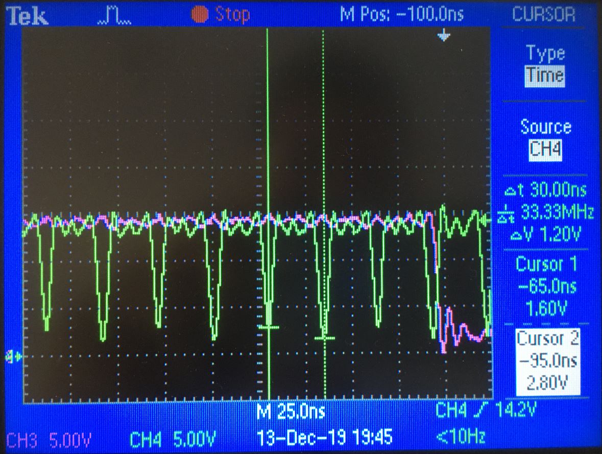
Green is the top gate signal

Pink is the bottom gate signal

I am baffled why I am observing sporadic 33.33MHz oscillations on the top gate when the bottom gate is high. This only occurs on only one of the 12 gate drivers. I have also bypassed the buffer with the same results.

  • Hi Tony,

    Thanks for your detailed post. If you hold the lower gate signal constantly low and only switch the high side, do you still observe the same error?

    Regards,

    Audrey

  • I am still observing the same error when I hold the lower gate signal low.

  • Hi Tony,

    Thanks for clarifying this point. Can you please share a schematic? Also, please note down the test conditions in the schematic, if possible.

    Thanks,

    Audrey

  • Buffer circuit on Power Board:

    Gate driver circuit on Controller Board:

    Test condition:

    • All gate signals are low except for uCPhase3_TG1
    • Gate signals are generated from a TMS320F280049 using the PWM module
    • Gate driver power supplies are generated via an isolation transformer and then regulated at 15V using a LDO
    • MOSFET internal resistance is 4R @ Tj=25degC
    • There are power supplies on both the Power Board and the Controller Board (<250kHz fs)
    • There is CAN module (250k), ADC module and GPIO currently enabled on the TMS320F280049 running at 100MHz
    • As already mentioned, this circuit is duplicated for 11 other gate drivers with no known issues

  • Hello Tony,

    Thanks for sharing. Have you done an A-B-A swap? Please replace the bad chip with a known good chip in the same position of the board to see if you observe the same issue. Also place the bad component in a known good region of the board, and see if the issue is still observable using the bad IC. If the failure follows the IC, then you may proceed with a customer return. If it does not follow the IC, then you may be observing a systemic issue. 

    Regards,

    Audrey

  • Audrey,

    I have ordered the ISO5851 instead of the ISO5451 which from what I can see, has a better CMTI. Can you confirm that I can replace the ISO5451 with the ISO5851? What is the functional difference between these two IC's?

  • Hi Tony,

    ISO5851 has higher CMTI and isolation ratings than ISO5451. Functionally, they are the same and you can replace ISO5451 with ISO5851.

    Were you able to resolve the previous issue? 

    Regards,

    Audrey

  • Audrey,

    To provide an update:
    - A new Controller Board and new Power Board was used. The Controller Board had new ISO5451 gate drivers.
    - I then replaced the ISO5451 with a new ISO5851 only on the problematic gate driver on one of the Controller Boards.
    - I swapped the Controller/Power Board configurations.

    The noise still appeared on the top gate signal on Phase 2 in all of the above conditions. There were no other gate signals present. I wanted to replace the TI gate driver with an Infineon pin-for-pin part as mentioned in the 'ISO5851: Can ISO5851 directly replace 1ED020I12-F2?' post however, my primary side rail is 3.3V instead of the rated 5V.

    There is another post titled 'ISO5451: Wrong turn-off signals' which shares similar gate signal behaviour to what I'm observing. The solution was taken offline. Can you advise the solution offered by TI?

  • Hi Tony,

    It is still not clear what is causing the issue.

    Is it only one of your gate driver boards that has this issue? In that case, it sounds like there is a systematic problem specific to this particular gate driver board (layout, soldering connection, etc). Or does it occur on every gate driver board?

    Do you have the VCE and IC measurements that you could share?

    Regards,

    Audrey

  • Audrey,

    To clarify, the DC/DC Converter comprises of a Power Board and a Controller Board. The Controller Board has the TI gate drivers and the Power Board has the IXYS buffer's. The schematic for these sections was shared in a previous post. I have two Controller Boards and two Power Boards. The noise issues occur on all Controller/Power Board configurations. The noise occurs on only one of the twelve gate drivers, namely the top gate of Phase 2. Understanding there could be a systematic problem with the Controller board (or the Power Board or both) which could be PCB layout related, unknown resonance occurring, ISO5451 issue, etc., I'm naturally trying to determine the root cause of the problem as this is preventing me progressing with development. The tests were done with no supply voltage i.e. left open circuit.

    With regard to the 'VCE and IC measurements', are you referring to the collector-emitter voltage and collector current? As mentioned in my previous posts, I'm using MOSFET's for all the switching devices. Please clarify your statement.

    Please respond to the question in my previous post and listed again:

    "There is another post titled 'ISO5451: Wrong turn-off signals' which shares similar gate signal behaviour to what I'm observing. The solution was taken offline. Can you advise the solution offered by TI?"

    I have provided some images comparing the similarities between the other group's issue and mine. The green waveforms are the gate signals in both oscilloscope images however, the ringing frequencies are different.

  • Hi Tony,

    Thanks for clarifying again. I mean to say VDS and ID measurement.

    In the other customer case, it seems this behavior is only occurring during load switching, and they were experiencing coupling issues due to high dv/dt. The ground planes of the primary and secondary sides of the IC should not overlap. They measured the input signals with differential probes and found noise at the input. They ended up adding filtering caps to the input pins (1nF and 100pF) to GND and a pullup resistor on IN- to VCC. However, since the issue you are seeing also occurs during no-load switching, then there may be another reason.

    How does the physical layout of this Controller board differ from the others? Is the controller board nearby any other coupling mechanism (ex supply transformer)? 

    Regards,

    Audrey