This thread has been locked.

If you have a related question, please click the "Ask a related question" button in the top right corner. The newly created question will be automatically linked to this question.

The bad load regulation at high line input (e.g. more than 220Vac)

Other Parts Discussed in Thread: UCC28780, LM5114, TL431

Hi, Technician or Manager,

I have designed a 65-W prototype by using UCC28780.  I found that at 90Vac input, the Vout only drops 0.07V when the load current increases from 0A to 3.25A.

However, when the line input voltage increases to 220Vac or 240Vac, the Vout drops nearly 0.9V from 0A to full load (3.25A).

I have tried to decrease the Ropp from 1kOhm to 250 Ohm, it does not work. and I tried to increase the Cout from 680uF to 1360uF, and the Vout also drops a lot at the high line input from 0A to 3.25A.

What might cause such problems? Could you give me some suggestions about how to solve it?  Thanks!

  • Hi Kailun, an expert will get back to you tomorrow. thanks.—— Teng

  • Hi Kailun,

    Could you please share the schematic for reviewing.

    Thanks.

  • Hi Teng Feng,

    Thanks for your in-time reply!

    Here is my schematic.

    Thanks! 

    65W_ACF_Schematic_Version 11H_wo Notes.pdf

  • Hi Kailun,

    I need more information about your design:

    1, If it's a 20Vout design ?

    2. how about the transformer magnetizing inductance Lm and Lk.

    3. Looks like your are using GaN FET , could you please share the part name

    4, Whether all of components value and P/N shown in the schematic are the same with you place on the board. special the opto-coupler  and feedback loop resistors

    5. please let me know the switching frequency when AC_in =90Vac  and 240Vac at full load.

    Thanks.

  • Hi Kailun,

    I need more information about your design:

    1, If it's a 20Vout design ?

    "Yes, it is a fixed 20Vout design, the maximum output power is designed to be 65W."

    2. how about the transformer magnetizing inductance Lm and Lk.

    "The primary inductance is around 116uH (Lm), the leakage inductance (Lk) is around 1.96uH."

    3. Looks like your are using GaN FET , could you please share the part name

    "I am using the GaN FET from GaN System, Low-side DUT is GS-065-011-1-L (650V-150m-11A), and the high-side clamp switch is GS-06-008-1-L (650V-225m-8A), with discrete gate driver (LM5114 from TI)".

    4, Whether all of components value and P/N shown in the schematic are the same with you place on the board. special the opto-coupler  and feedback loop resistors.

    "Yes, All of the components value and P/N shown in the schematic are the same with their place on the board".

    The feedback loop resistor value is the same as the schematic, the optocoupler is FODM8801AV.

    5. please let me know the switching frequency when AC_in =90Vac  and 240Vac at full load.

    The switching frequency at full load is around 197kHz at Vin=90Vac, 214kHz at Vin=115Vac, 267kHz at 220Vac, and 247kHz at 240Vac.

    In addition, I would like to consult whether I could make a loss breakdown analysis about this active-clamp flyback topology, including the loss in the diode bridge, power devices, and synchronuous rectifier. Could you recommend some methods or simulation method for me? Thanks a lot.

    Thanks.

  • Hi Kailun,

    I have reviewed your schematic. and I don't see too much need improvement. could you please try to minor increase Rcomp from 551k to 750k OR 1M

    For a little bias current out from FB pin , and decrease Rbias1 from 8.25k to 5k for a little higher DC gain . also decrease Rbias3 from 34K to 20k .

    For the loss breakdown analysis , I suggest you download the Mathcad calculation tool and Simplis simulation model from TI.com in below link:

    https://www.ti.com/product/UCC28780/toolssoftware. Hope that can help you.

    Thanks.

  • Hi Jaden,

    Thanks for your reply!

    I have tried to increase Rcomp from 551k to 1M, but it does not work.

    For Rbais1 (8.25k) and Rbias3 (34k), I still keep the same.

    I found that the drop of Vout is due to the drop of Vref, and after adding a parallel capacitor with the Ro3 (21.5k in the schematic, it is changed to be 21.76k to make the Vout equal to 20V) the following is the measured data under the full load (20V-3.25A). 

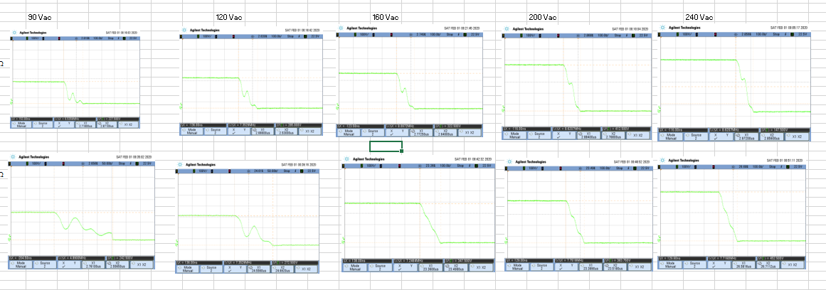
    Here is another problem that I would like to consult you. The following is the measured waveform of Vsw at the full load (20V-3.25A). In this test, I add a Csec=1980pF at the secondary side of the transformer (S-F). The upper row is the waveform without Csec =1980 pF, and the lower row is the one with Csec =1980pF.

    You could see there is always some ring of Vsw. I would like to consult the reason for this phenomenon, and how could I understand it and then solve it?  Thanks!

  • Hi Kailun,

    I don't agree your description "I found that the drop of Vout is due to the drop of Vref". because Vref is a input signal for TL431 . but after you add a Cref between Ref and GND, the output is more stable . what I can guess is the PCB layout on your board is poor.  when at high line input and heavy load, the sharp DV/DT or DI/DT cause large noise coupled to the Ref PIN of TL431 , but if added a filter caps on it . get more better . general speaking , we don't suggest add this filter cap. in here , since it will delay the loop response. So you maybe have to improve your PCB layout in here.

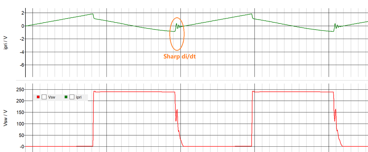
    About your second question , this Vsw ringing is a normal behavior. it's caused by Non-ZCS turn off SR FET , in other word , when high side FET turn off. the resonance current didn't touched demagnetizing current . caused a sharp di/dt on primary side , this sharp di/dt on leakage inductance will lead to a voltage rise . V=Lk*di/dt , if you decrease the secondary resonance caps Co_2,Co_a .. and primary side clamp caps Cclamp1---2--3 , the resonant period will be shorter.

    that means the resonance current will be touched the demagnetizing current . SR FET will ZCS turn off , then you will not see this ringing happens .

    But I don't suggest to do it .because the negative resonance current becomes an extra current source to discharge the high capacitance region of the high side FET COSS curve in addition to negative demagnetizing current. that is benefit for efficiency improvement.

    And I it's not necessary to add a 1980pF cap. on XFMR secondary winding.

    Attached my Simplis simulation waveform for your reference.


  • Hi Jaden, 

    Sincerely thanks for your detailed reply.

    For the first problem:

    I still could not understand how the primary side dV/dt or di/dt could be coupled to the secondary side. Does it realize through the 2200pF Y-cap or Transformer?

    I would try to improve my PCB layout to avoid the noise coupling to the REF pin.

    For the second problem:

    I found this ringing of Vsw would result in a noticeable switching ripple on the Vout (around 200mV).

    The following screenshot is the Vout measured by the differential probe. (even I use the 10:1 low-voltage passive probe and use the short ground tip, the switching ripples still exist). 

    Therefore, I would like to mitigate this kind of ringing of Vsw. I have tried to adjust Rtz and Rdm, and found that too large Rdm would make the system unstable and make it easier to trigger OPP at high line input. 

    I could decrease the Clamp or Co2 to shorten the resonant period, but the resonance still exists. How could I totally mitigate it in my board? Could you give me some further suggestions?

    Thanks !

  • Hi Kailun,

    Firstly, make sure you had measured the ripple correctly , I suggest you don't use differential prober but normal prober to measure the ripple.

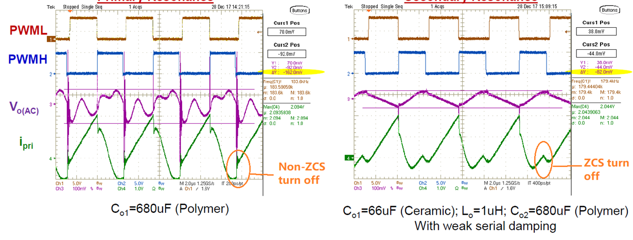
    Non-ZCS turn off of SR FET will lead to more higher ripple noise on output , as I suggested , you have to decrease primary and secondary side resonance caps to let SR ZCS turn off , how you can judge what capacitance are ok for the ZCS , I propose you capture the transformer primary winding current , this signal can tell you if your resonance capacitance are proper or not . show as in below image:

    BTW: It's not necessary to adjust RDM and RTZ once them were correctly set by your design at the beginning of your debug . the wrong setting of RDM will delivery wrong message to the controller and lead to unpredictable issues. please check the datasheet of how to set RDM and RTZ.

    I Strongly suggest you to read the datasheet for better understanding the UCC28780 control strategy and ACF topology , I also attached some papers for your reference.

    Since lots of questions asked in this post, we have timeline to close the post . if you have further questions about ACF and UCC28780 Please feel free to create another post.

    Thanks.

    3_Comparison of GaN and Silicon FET_5Dec_KM.pdfActive Clamp Flyback Using GaN Power IC for Power Adapter Applications.pdf

  • Hi Jaden,

    I would try your suggestion and thanks for sharing the related materials with me.

    Sincerely thanks for your patient reply!