Hi,
I'm struggling a bit with a design based on the LM5069 as a high side load switch controller. I'm controlling the LM5069 by applying voltage to the UVLO pin. If I switch the output on with no load, the voltage comes up and I can then apply load with no problem. If, instead, the load is connected to the circuit output and I apply voltage to the UVLO pin, the circuit does not bring the output up.
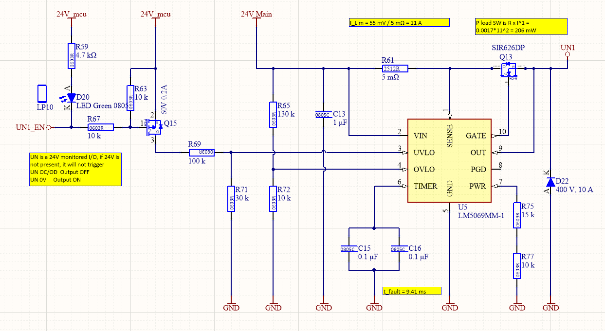
I have designed the circuit using the design calculator and simulated it in TI-TINA but my built circuit doesn't match the simulated behaviour. I've tried with and without the dv/dt additional circuit and got the same behaviour.
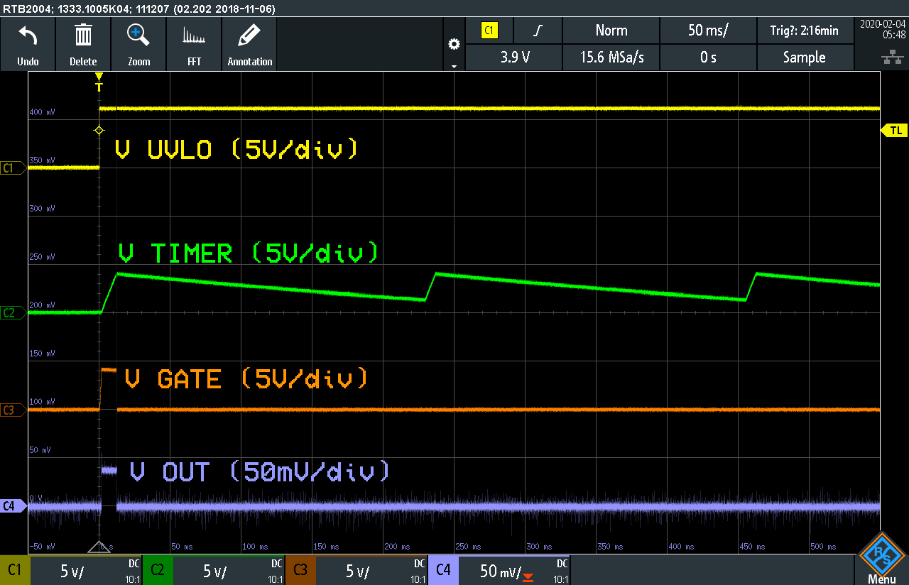
Using an LM5069MM-2, the voltage on the timing capacitor rises at about 80 µA, which I understand to mean an over-current or over-power fault is detected. However, the voltage across my 5 mΩ current shunt never seems to go above 10 mV and my supply voltage is ~28 V. My power resistor is 25 kΩ and I measure ~500 mV across it when the controller is trying to switch the output on. It seems like the LM5069 is regulating the gate voltage down to limit maximum power but to a point much lower than what I've set with the RPWR.
As shown in the waveforms, the controller seems to try the output once, then continues to automatically restart detecting a fault. After the first attempt, the restarts are not accompanied by gate voltage or current flow, so I'm not sure what is making the controller think there's a fault.
I appreciate that the controller is really designed for protecting a system when the input power is connected and disconnected, rather than as a load switch with constant input power but I didn't think I'd be too far outside the intended design use with my application. I'm essentially trying to replace relays and fuses with semiconductor switches in an auxiliary 24 V automotive system. I'd like to switch up to 55 V, and different loads I have require current "fusing" at 3 A, 7.5 A, 11 A and 15 A. Is the LM5069 suitable for this, or if not, is there another product you'd recomend?

1033.LM5069_Design_Calculator_REV_C.xlsx