


Other Parts Discussed in Thread: TPS7A52
Hi,
we need to vary PA output of a certain FEM.
This chip is currently (its a given design, in production) sourced by 3.3V - which is neccessary for max PA output. To achieve lower output I need to reduce VCC_TX, e.g. in 4 steps between 1.5 - 3.3 V. My plan is to to vary R2 between certain values, using e.g. solder bridged parallel resistors:

But: VIN is 3.3V and VOUT needs to be 3.3V in case of max PA. Am I allowed to bridge VIN with VOUT in that case without damaging something?
Same question on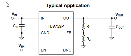
thx
GGA

