This thread has been locked.

If you have a related question, please click the "Ask a related question" button in the top right corner. The newly created question will be automatically linked to this question.

LM5022EVAL: Transformer Capacitance & Slope compensation stabilisation

Part Number: LM5022EVAL
Other Parts Discussed in Thread: LM5022

Hi,

I'm designing a flyback using the LM5022

VIN: 30V to 600V

VOUT: 15V 2W

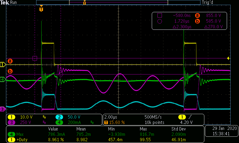
  • CH1: VGS Q102 (principal sw)
  • CH2: VAK D4 (output diode)
  • CH3: VDS Q102
  • CH4: iDS Q102

2 questions:

  1. VIN=400V, LOAD=103R0. the inrush current at the turn ON of the MOS is principaly due to transformer capacitance ? So to limit the peak current, a "new" winding is recommended... any suggestion ?
  2. I'm not able to have a stable PWM at low voltage (i.e. 60V), is there a "clean" way to select components to avoid this ? I think it's start with a good slope compensation.

tidrui5 (SCH) solution 3.pdf

  • Hi Alexandre,

    Thank you for using the LM5022. The current spike is mainly the reverse recovery currents of D4, and also D105, plus the gate drive current. Transformer capacitance has very little contribution here. 

    C105 is too big.  Please choose 0.001uF.  See if this stabilize the PWM operation.

    Your connection between D105 and D6 (shown in your schematic markup) basically break the isolation boundary.  Recommend to use R110 and R111 to directly  sense VOUT for output regulation.  Namely, remove D105, and connect D4 Anode to D105 Anode.   

    Thanks,

    Youhao Xi, Applications Engineering