This thread has been locked.

If you have a related question, please click the "Ask a related question" button in the top right corner. The newly created question will be automatically linked to this question.

CCS/TPS650061: TMS320C6748

Part Number: TPS650061
Other Parts Discussed in Thread: TMS320C6742, , TMS320C6746, TMS320C6748

Tool/software: Code Composer Studio

Hi 

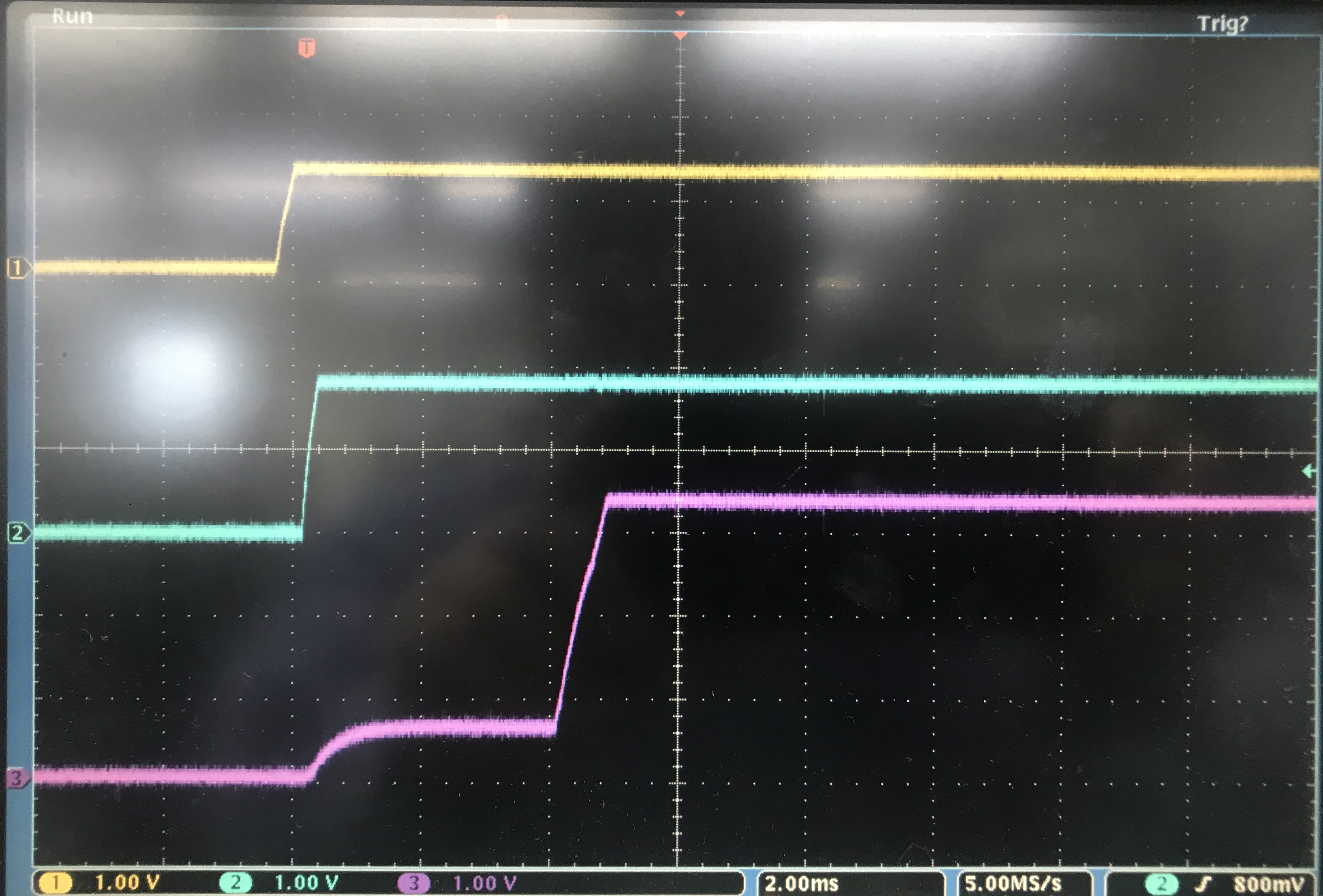
The circuit was designed as shown in Figure 1 with reference to “SLVA490–October 2011, Powering the TMS320C6742, TMS320C6746, and TMS320C6748 With the TPS650061”, but the turn on time of 3.3V is 3.7ms + 900us (Figure 2). I understand that the 3.7ms delay is due to the TPS3805's sense resistors (R6, R8) and capacitor (C12), but I don't understand what the 900us Ramp Time is. SLVS810C's VLDOx Ramp Time is typical 200us and there is no Min / Max value. Do you know how much Min / Max is? And can you see why about 900us Ramp Time occurs?


Figure 1, TPS650061 Circuit


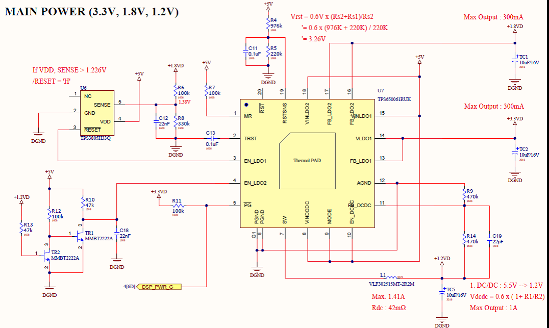
Figure 2. TPS650061 Power-On, Ch1 : 1.2V, Ch2 : 1.8V, Ch3 : 3.3V


Regards

Oh

  • Hi Oh,

    Min/Max specifications for the output ramp times are not tested or characterized on this device. However, a typical or average unit should have a 200 us ramp time on the LDO output under the operating conditions specified in the datasheet. 

    1. Have you observed this ramp time on multiple units?
    2. Do you have any additional capacitance on the +3.3VD rail? If there is enough capacitance to trip the LDO current limit (min. 340 mA), the output ramp time will increase. 

    Thanks,

    Gerard

  • Hi Gerard,

    Thank you for your reply.

    I observed this ramp time on multiple units. 

    It has an additional capacitance of approximately 100uF on the +3.3VD rail.

    This additional capacitance is the decoupling capacitance of other devices. 

    Thanks.

    Oh.


  • Hi Oh,

    In that case the operating conditions no longer align with the datasheet, which assumes only the components specified in a typical application (10 uF LDO output capacitor). As a result, some datasheet specifications, such as the LDO output ramp time, are subject to change.

    With additional decoupling capacitance, the increase in ramp time is expected. The +3.3VD rail will draw a lot of current on start-up to charge the large decoupling capacitors. The LDO short-circuit current limit feature limits this inrush current to a constant value to prevent damage to the device. With a constant inrush current, the output ramp time will scale linearly with the capacitance on the +3.3VD rail:

    Isc = C * dV/dt => dt = C * dV / Isc

    Assuming the minimum case for the short circuit current limit (Isc = 340 mA), the output ramp time can be approximated as:

    dt = C * dV / Isc = 100 uF * 3.3 / 340 mA = ~970 us

    Thanks,

    Gerard