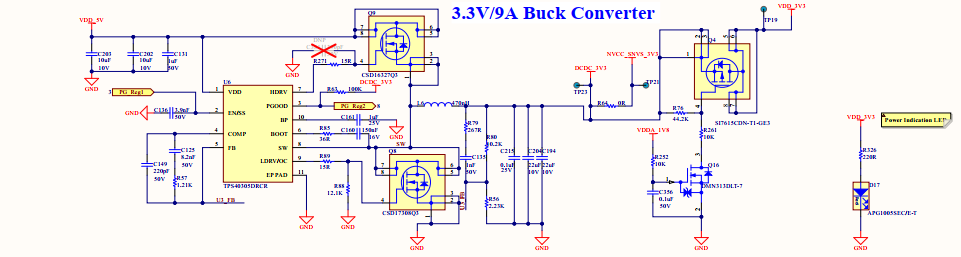
This thread has been locked.

If you have a related question, please click the "Ask a related question" button in the top right corner. The newly created question will be automatically linked to this question.

TPS40305: 3.3V Switcher EMI issue

Part Number: TPS40305

Hi TI Team,

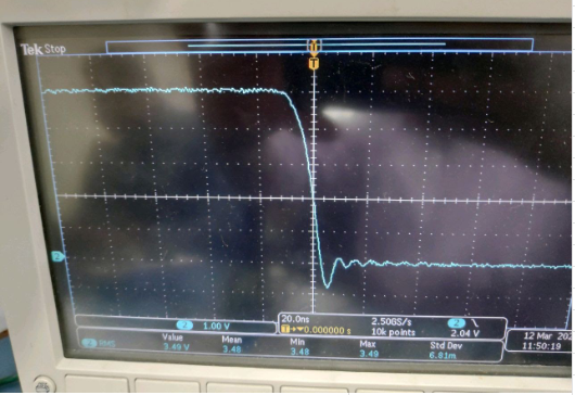
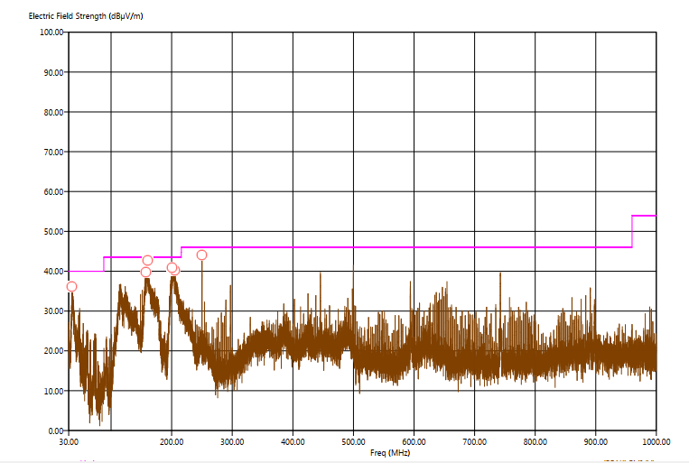
We are using TPS40305 switcher with 5V input and 3.3V, 9A output.  We are facing issue in pre-compliance test (FCC Part 15B). We are getting out of limit 160MHz broadband noise. Can you please help on reducing this broadband noise? 

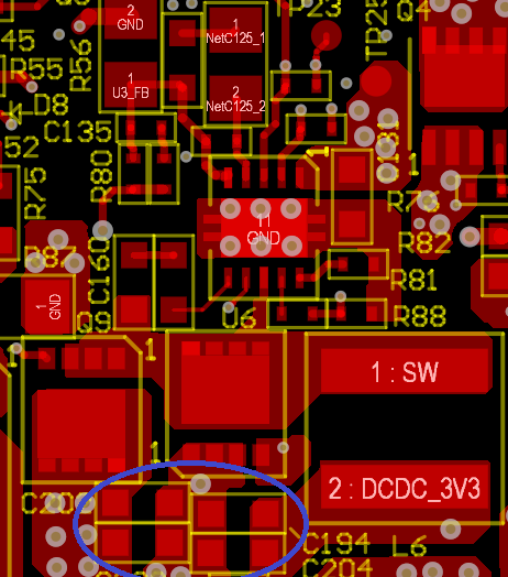
Attached is the snapshot of schematic and placement & routing.

  • Hi Sahil,

         Anyways, one obvious thing that I could see is that the snubber resistor and capacitor should be placed on the SW node side of the inductor (meaning the side of the inductor where the FETs are connected). The schematic shows connection to the output side of the inductor which makes the snubber practically useless. This could significantly help with ringining and hence your EMI.

    Also, can you share you spectrum plot for the EMI tests to get some insight into how much noise we have?

    Regards,

    Gerold

  •  

    160MHz noise is almost certainly related to the switch-node ringing when the FETs are turned on or off.  This occurs because the parasitic inductances in series with the FETs ring with the parasitic capacitance of the switch-node to produce a resonant oscillation with very high frequency.

    Your schematic shows 3 input capacitors, 2x 10uF and 1x 1.0uF.  None of these are particularly good at bypassing the input voltage at 160MHz.  I can see the 2 10uF capacitors, (C202 and C203) but I don't see C131, the 1.0uF capacitor.  Since there are vias to both the drain of the high-side FET and the source, it would help to move one of the 10uF bypass capacitors to the backside of the board populate an 2.2-10nF 0402 capacitor where C202 is located to provide better high-frequency bypassing of VIN to GND.

    Adding a snubber to the SW node (series resistor can capacitor) can help dampen the ringing of the switch node by absorbing the energy before it can radiate.  Here is a link to designing a snubber based on lab measurements of the parasitics:  https://e2e.ti.com/blogs_/b/powerhouse/archive/2016/05/05/calculate-an-r-c-snubber-in-seven-steps As Gerold notes, the snubber needs to be off of the switching node.  Gerold mistook the compensation components as bring connected to ground and thought those were your snubber (R79 and C135)

    Your gate drive and boot strap resistors (R271, R89, and R85)  appear to be set-up to slow down the switch node and reduce the ringing, but they may be too large to be effective, especially R85 at 36-Ohms.  These could be so large that they are pinching off the gate drive during start-up and actually increasing ringing rather than decreasing it.  I would recommend trying to reduce these to 2.2-ohms and see if that helps in combination with the snubber and input bypassing.

    The traces connecting these pins to the IC are also really thin.  While that is likely unrelated to the noise issue, it would be good practice to widen these traces to to at leas the 0.2mm width of the IC pin.

    How much do you need to reduce the 160MHz noise?

  • Hi Gerold/Peter,

    Thank you for your response.

    We had recently captured SW node waveform to check whether there is ringing or not. I have one waveform which I am attaching for your reference. We didn't observed any ringing except a voltage dip as seen in attached snapshot.

    Also, C131 is placed right near the TPS40305 IC pin.

    We have actually reduced ringing by adding gate drive and boot strap resistors.

    Also, please find the attached spectrum plot for your reference.

  • Hi Team,

    Any update on this?

    Any feedback on previously attached waveforms??

  •  

    Thank you for the waveforms.  Yes, the turn-off appears to be quite slow and smooth with about 10ns fall-time and minimal resonate ringing at turn-off.  The concern with such high HDRV and BOOT resistances is more on the rising edge of the SW node where the high-side FET is turning on, if the gate-drive current is too limited, it can cause the FET to turn-off as the Drain to Source current pulls the SW node up and collapses the Gate-Source voltage.  That can cause the switch-node to oscillate as the switching node rises.  If you've checked that and the rising edge of the switching node has a similar 10ns rise time, when under load, it would seem that the switching node is not the culprit, and there is some other element in the circuit resonating at this high frequency.

    Are you able to move the radiant EMI probe around the design to try to identify where the peak noise is coming from?  If not, you can build your own radiant loop probe by wrapping some bare wire around the metal ground barrel of an oscilloscope probe and then looping the end back to the probe tip.  Then, with the oscilloscope running, move the looped probe tip around the circuit to try to identify the peak location for the problematic noise.

    You said C131 is close to the IC.  That is providing filtering to the input voltage to the IC, but not bypassing of the input voltage to the power FET Q9/Q8.  With only C202 and C203 bypassing the Q9 drain to Q8 Source, we could be seeing ringing at the VIN node at the FETs and ceramic bypass capacitors.  I calculate about 4.3A of input RMS ripple current on the input capacitors, which is a lot just 1 10uF input capacitor, but as an experiment to see if this is the issue, can you try removing C202 and soldering it on top of C203, then installing a 10nF 0402 capacitor where C202 is located, shifted as close to the drain of Q9 and Source of Q8 as possible to see if that reduced the noise generated by the pulsed load current on VIN?

    Another possible source for high frequency radiated noise would be the 5V input trace.  Is there any higher ESR bypass capacitors, such as bulk electrolytic capacitors, from 5V to GND close to the C202/C203 input capacitors?  Is there a ferrite bead in series with the 5V input?  These circuit elements help contain high-frequency noise close to the converter to limit their antenna area to radiate that noise into the surrounding area.

  • Hi Peter,

    Thank you for your response.

    We saw maximum peak noise coming near the C202 & C203 capacitors as highlighted in the attached snapshot.

    We will perform the test by adding a 10nF cap as suggested by you and get back to you with results.

    Also, we don't have electrolytic capacitor on 5V rail near C202 but we do have one 47uF ceramic capacitor as highlighted in the attached snapshot. Also, we don't have any ferrite bead. 

  •  

    That sounds like very good progress.  Let me know how the tests go.

    Is there space on the backside of the PCB to place a capacitor between the VIN and GND vias  at the Q9 Drain and Q8 Source.

    Another possibility would be to split the self-resonance frequency of the two input capacitors C202 and C203 by changing C203 from 10uF to 22uF and C202 from 10uF to 4.7uF.  By splitting their self-resonant frequencies, they can help dampen and suppress noise each device is generating.  If there is space to put capacitors on both side of the PCS, it would be best to place the 2.2-10nF capacitor closest to the FETs, the 4.7uF next closest and the 10uF or 22uF on the backside of the PCB so that the highest frequency capacitors have the least inductance to the Power Fets.

  •  

    Have you ran the additional tests?

    How is the performance?