This thread has been locked.

If you have a related question, please click the "Ask a related question" button in the top right corner. The newly created question will be automatically linked to this question.

TPS61236P: TPS61236P Output Voltage Issue.

Part Number: TPS61236P
Other Parts Discussed in Thread: TPS61022

Dear TI Team,

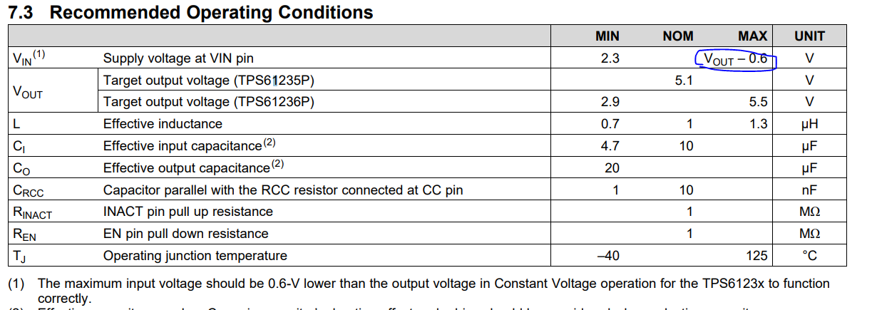
If the difference between the input voltage and the output voltage of the TPS61236P is designed below 0.5V, can you know what kind of damage it does to the IC?

VIN: 4.2V
Vout: 4.5V 1A

In the above design, short defects of SW pin and VOUT pin occur about 5%.
(Chip Only Impedance SW to VOUT pin: about 22ohm)

I want to check if the cause of the defect is due to the voltage difference between Vin and Vout.

Best Regards,

Thanks.

  • Hi Youngsu,

    Per datasheet part 7.3. The maximum input voltage should be 0.6V lower than the output voltage.

    You may choose another boost device which can support Vout-Vin<0.5V. For example, TPS61022 is a good choice.

  • Hi Liu,

    We confirmed that the design is not satisfactory.
    I want to know what can happen if the voltage difference between Vin and Vout is less than 0.6V.

    Thanks.

  • Hi Youngsu,

    During CV operation, the maximum VIN should be 0.6-V below VOUT to keep the output voltage well regulated. The TPS6123x may enter into pass-through operation prematurely when VIN is close to but still below VOUT, and exists when VIN is below the threshold with a hysteresis. When in pass-through operation, the boost converter stops switching and keeps the rectifying switch on, so the input voltage can pass through the external inductor and internal rectifying switch to the output. The output current capability becomes lower and is limited by the precharge current limit ILIM_pre of the rectifying switch. More than 0.4-V under-voltage of VOUT may occur due to the premature pass-through operation and the hysteresis of existing. If the under-voltage is not acceptable, the maximum VIN should be limited to 0.6-V below VOUT , which gives enough margin to avoid the pass-through operation.

    To find the root cause of short defects of SW pin and Vout pin, please share the schematic and layout. Also share the key waveforms if you have,

  • Hi Liu,

    Share the layout.

  • Hi Youngsu,

    The layout is not good. 

    1) The output capacitors placement is not recommended. TI suggests place the output capacitors close to the IC. The capacitors are directly connected to Vout pin and GND pin so that the PCB parasitic inductance is the minimum. With the below placement, the big parasitic inductance will cause high spikes at SW nodes and even cause damge.

    2) The FB gnd should be the AGND.

    Why do you say TPS61022 is not satifactory?

  • Hi Liu,

    Thank you for your confirmation.

    MP starts and cannot be changed.

    I am considering a way to increase the output voltage.

    Best Regards,

    Thanks.

  • Hi Youngsu,

    I suggest you to optimize the layout because otherwise it's not easy to solve the failure issue.