This thread has been locked.

If you have a related question, please click the "Ask a related question" button in the top right corner. The newly created question will be automatically linked to this question.

UC3825: To configure the Error amplifier

Part Number: UC3825

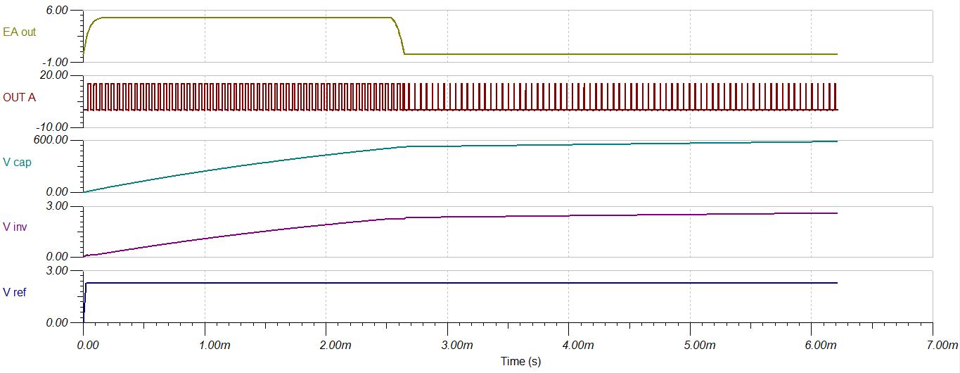
In my application,i want to charge the capacitor to various voltage levels(100 to 500V) through a full bridge inverter and diode bridge rectifier.The output pulses(Out A and Out B) of the UC3825 are given to the inverter.

So,I want to make the output pulse of UC3825 to be completely zero once the output voltage reaches the reference voltage(pin 2).So,how to make the error amplifier to work like this.

  • Hello Gopinath,

    Thank you for your interest in the UC3825 PWM controller.

    The output of the error amplifier is compared to the RAMP signal at a comparator to generate the PWM duty cycle. The RAMP signal has a 1.25V offset built-in, so when RAMP = 0V, the comparator positive input will still be 1.25V (1.1V minimum, per the datasheet). 

    You can achieve zero duty-cycle whenever the error-amp output voltage is less than 1.1V.  This requires the error-amp negative input to go slightly higher than the reference input (pin 2), to drive the error voltage down.

    Regards,
    Ulrich

  • Vinv(pin 1),Vref(pin 2=2.5 V),Vcap(Where i want to charge the capacitor at 500 V),Vramp(from Ct-Timing capacitor(1V to 2.8V))

    I have simulated my application circuit in TINA.I have set the Vref(pin 2) and my capacitor starts charges.After the capacitor reaches its reference voltage,EA out becomes zero but the output pulses from OUT A is not becoming zero(you can able to see the difference after EAout becomes zero) .Due to this minimum pulses after EA out attaining zero,the output capacitor charges even after attaining its reference voltage.Can you tell me about this problem?

  • Hello Gopinath,

    That is not the expected behavior of this controller.  There must be something wrong with the TINA model of the UC3825 device. 
    Consider that if it is not able to go to 0% duty-cycle, all of the thousands of applications using this part over the past decades would have gone to over-voltage at some load condition. It would be a useless part. 

    The fact that it has been a very successful device indicates that the problem is in the device TINA model, not the device.
    I will notify the appropriate group of this issue, but I can't predict when it will be fixed.

    To get around this problem in modeling, I suggest to add a set of external gated buffers to outputs A and B that can be disabled by a comparator monitoring E/A OUT.  When E/A OUT falls below (RAMP + 1.200V), the comparator will disable both output buffers so duty-cycle will be zero. 
    This essentially duplicates part of the internal circuitry that inhibits the outputs, but does not interfere with the ILIM and Soft Start functions.  
    I suggest that the off-threshold to be 50mV lower than the internal (RAMP + 1.25V) so it should not interfere with normal PWM operation at very low duty-cycles.  This external over-ride should only function when E/A OUT falls lower than the expected internal cut-off level.

    Regards,
    Ulrich

  • Thank you for this information.

    Is there any possibility to remove the internal 1.25V from the ramp?

  • Hello Gopinath,

    The internal 1.25-V offset voltage cannot be removed from the actual device of course, nor from the device model.  However, you may add an external -1.25-V DC voltage source in series with the RAMP pin in the simulation to cancel the +1.25-V internal offset.  In a real circuit, adding a negative offset circuit is more complicated to achieve, but the principle is the same.

    Regards,
    Ulrich