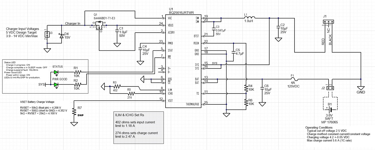
I would appreciate your review of the attached schematic and comments/answers to the following details that arose during the design process.
- Given circuit will be used with generic 5 VDC supply input rather than USB power is it correct to leave D+ and D- as floating?
- For non-USB operation is it correct that OTG and CE pins are grounded?
- Leaving VSET floating sets battery charge voltage to 4.208 VDC.
- What sets the voltage at which the BQ25616 disconnects the battery from load pending connection of charger voltage? Is the following correct?
- VBAT_DPL the BAT depletion falling threshold to turn off BATFET VBAT is specified as 2.18 min to 2.62 max V therefore the BQ25616 will disconnect the battery from SYS connected load at some voltage within that range.
- The pack to be used with BQ25616 based circuit has a protection circuit featuring voltage lower limit cutoff specified as 2.30 ± 0.050 V.
- Given the pack’s protection circuit cutoff voltage is within the range of BQ25616’s VBAT_DPL is there a danger the two circuits will trip each other into misbehaving? With no voltage present on VAC/VBUS pins two scenarios as battery reaches discharge state come to mind.
i. Pack’s circuit disconnects cell first, BQ25616 has no voltage source so at VAC/VBUS or BATT pins so it goes dark and cannot further effect pack until charger is plugged in.
ii. BQ25616 circuit disconnects cell first above pack’s 2.3 V trip off point, as per datasheet section 9.3.9.5.2 Battery Over-Discharge Protection. While pack supplies voltage to BATT pins the BQ25616’s Iq_bat quiescent battery current of circa 9.5 uA remains as a load on the pack. Thus eventually that uA load along with the cell’s self-discharge will eventually reach the pack’s 2.3 V trip off point. Stability depends on BQ25616 keeping battery disconnected from load as voltage on BATT lingers between 2.62 and 2.3 VDC.
5. Datasheet sections 10.2.1.2.1 Inductor Selection, 10.2.1.2.2 Input Capacitor and Resistor, and 10.2.1.2.3 Output Capacitor all use formulas that are a function of the switching frequency duty cycle. Prior to building a circuit and bench testing how is the duty cycle to be known? WEBBENCH or Tini-TI models do not appear to be available for simulation. Failing that the values used in datasheet and BQ25616EVM schematics were used. Are these sufficient or should they be checked against some range of duty cycles? If so what % range of 1.5MHz?


