This thread has been locked.

If you have a related question, please click the "Ask a related question" button in the top right corner. The newly created question will be automatically linked to this question.

LMG1205HBEVM: MOSFET blow up during load testing

Part Number: LMG1205HBEVM
Other Parts Discussed in Thread: ALLIGATOR

Hello,

MOSFET blow up during load testing, I have below questions:

1- Vpp was between -2.5 and +2.5, that could be an issue to blow up Mosfets? PS: Mosfet was working for testing current from 1 to 10 ampere then suddenly blow up and it happened for 2 kit boards.

2- I use DC power supply (Agilent N5747A) during the test i read Vin=40.01V, Iin=0.4A (the current that shows on power supply), duty cycle=40%, Vout=15.82V and Iout=1A. I used DC load. so in this case Pout=Vout*Iout is bigger than Pin=Vin*I in??? how it happened? i know efficiency should be around 90-95% depends on load current.

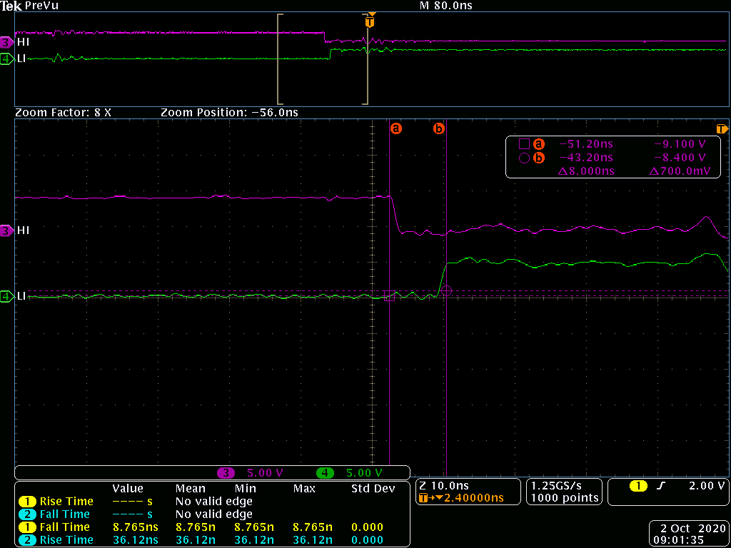
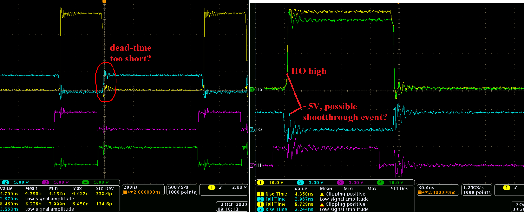
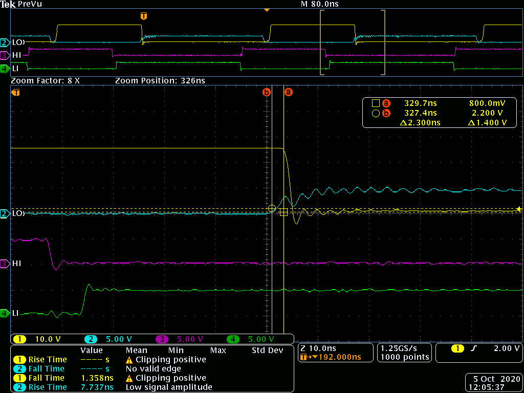
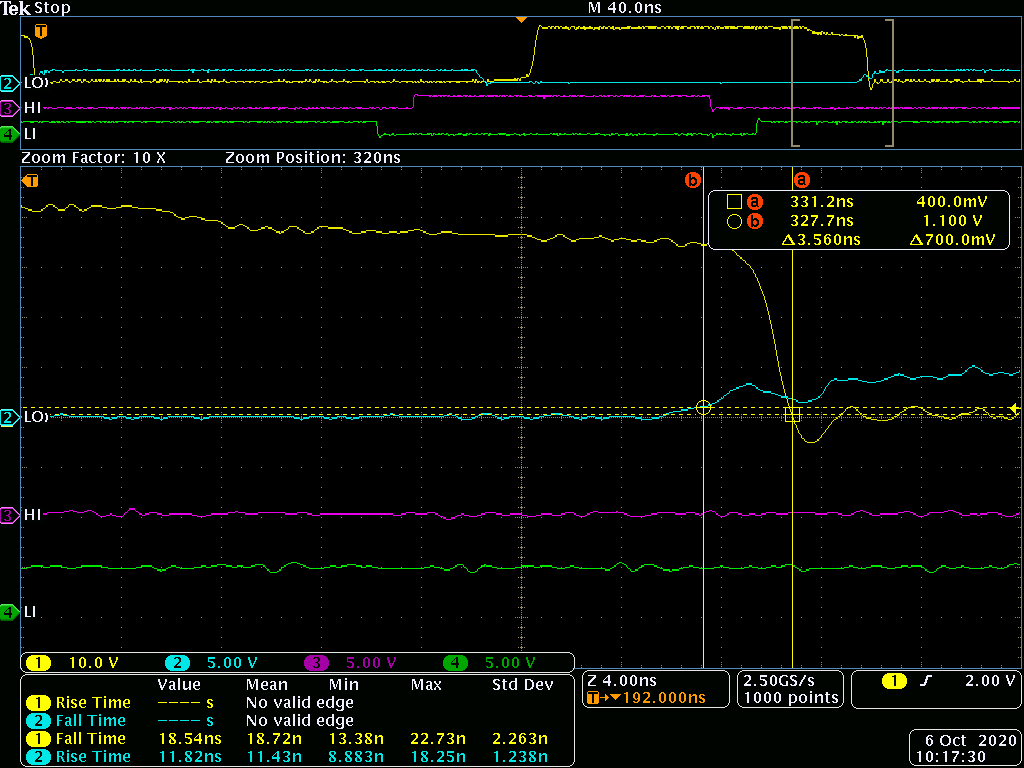
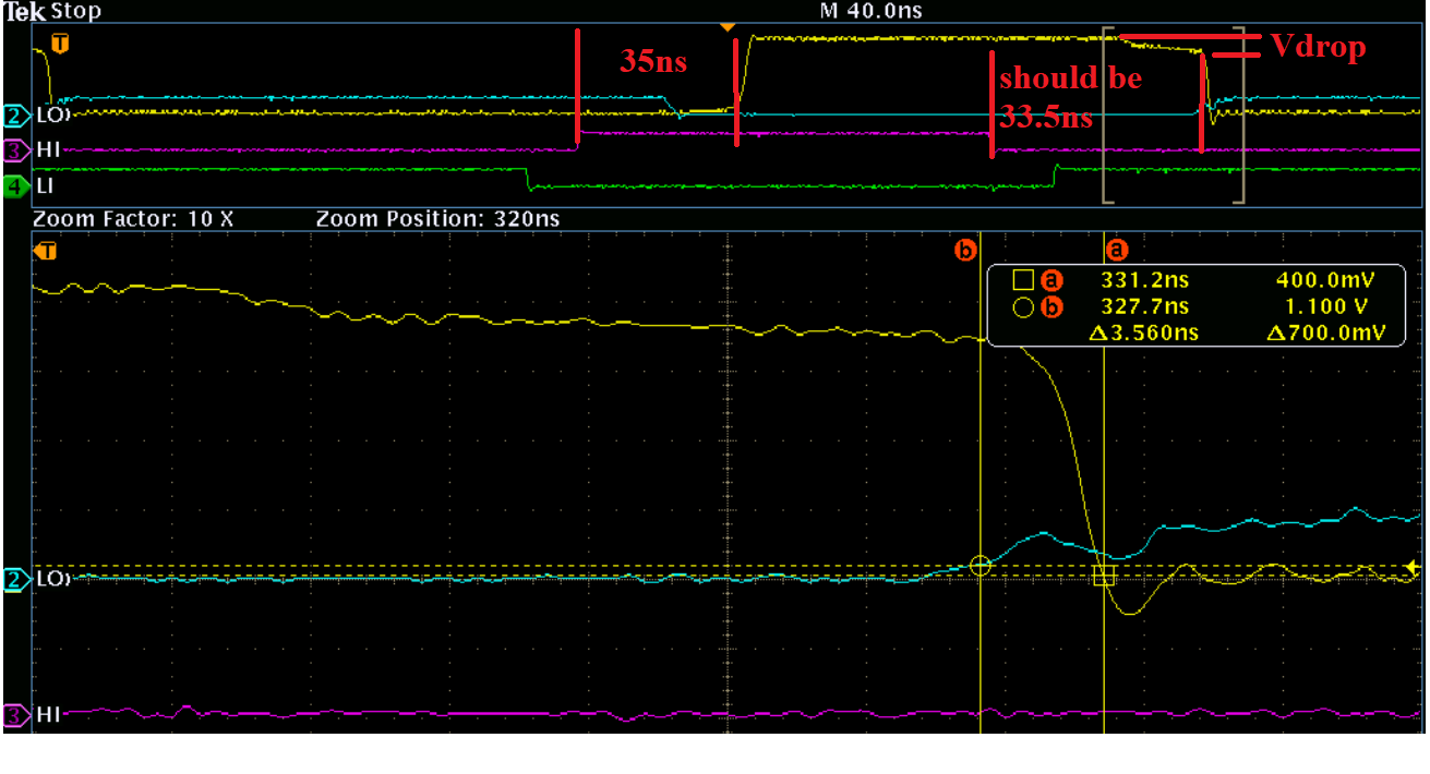
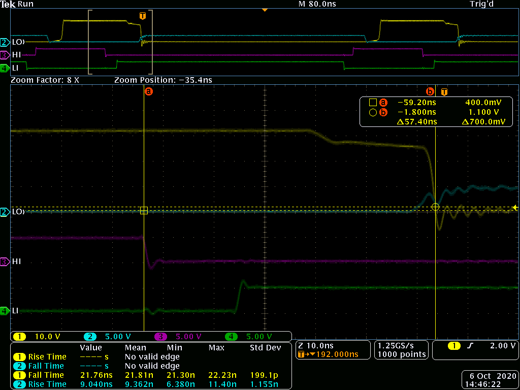
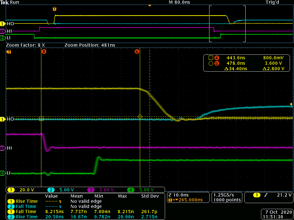
3- I calculate dead time on oscilloscope, with no load and without any Vbus. from HS fet-off to LS fet-on dead time is 1.5ns and  from LS fet-off to HS fet-on dead time is 4ns, is it on the range? I didnt change anything on the kit LMG1205HBEVM.

4- How long we could work with no load on the LMG1205HBEVM, without any damaging the kit? like around 2 or 3 hours should damage it?

Thank you!

  • Hello,

    Thanks for your interest in our driver.

    Do both MOSFETs fail? The Vpp measurement that you mentioned, is this the voltage captured at the gate of the FETs? If so, can you please clarify which FET?

    How are you measuring this voltage? I ask because probes with long GND leads might introduce additional parasitic and impacting the gate waveforms? Can you confirm that you're using tip & barrel method?

    I assume you're using the EVM with a single PWM input single in which case, you should be measuring 8ns dead time on HI and LI, can you confirm that this is the case? Can you also confirm that your waveforms at no load compare to Figure 11 on the user's guide?

    If possible (on the same image), can you please share your waveforms of input signals HI and LI as well as output signals HO-HS and LO-GND?

    The output power should not exceed the input power under normal circumstances and 

    So long as the operating conditions are within the specifications in Table 1, the EVM may operate at load without damage. Can you please clarify, I thought from the thread title, the failure occurred with the load connected? Please confirm and share any available waveforms of both input and output signals at no load.

    Regards,

    -Mamadou

  • Hello,

    Thanks for your quick response:

    Do both MOSFETs fail? The Vpp measurement that you mentioned, is this the voltage captured at the gate of the FETs? If so, can you please clarify which FET?

    Yes, both Mosfet blow up on each board, No Vpp is input PWM voltage, HI and LI voltage had some unstable wave at beginning but not minus voltage. FET type: EPC2001C

    How are you measuring this voltage? I ask because probes with long GND leads might introduce additional parasitic and impacting the gate waveforms? Can you confirm that you're using tip & barrel method? NO, i use scoop prob and GND but its short GND alligator connected to prob.

    I assume you're using the EVM with a single PWM input single in which case, you should be measuring 8ns dead time on HI and LI, can you confirm that this is the case? Can you also confirm that your waveforms at no load compare to Figure 11 on the user's guide? Yes, I used single PWM input, I thought we should calculate dead time on the HO and LO signal? but if its between LI and HI then it should be file according to below pic:

    Here is no load for 40V input at 1Mhz and 0-5 Vpp PWM input, yellow is HO: This is for new board I received, I dont have previous wave with -2.5/+2.5 (Vpp pwm). It looks that on the nno load on manual fig 11 HO and LO have the same amplitude but I have Vbus value on the HO on no-load condition?

    If possible (on the same image), can you please share your waveforms of input signals HI and LI as well as output signals HO-HS and LO-GND?

    Here it is, yellow is Ho and green Hs, on no load and Vbus=40V, Duty 30%, F=1MHz, does the waveform looks normal?

    Failure happens on the load condition, but I created same connection and configuration for new board with same instruments. is the condition looks right?

    Could I use the board for no load and load for about hours without any damage? What do you think was the issue?

  • Hello,

    Thanks for the additional waveforms.

    From the waveforms you shared, there are several instances of possible shoot-through specifically on falling edge of HO and rising of LO (of the second waveform), could you please share zoomed in waveform of that section?

    The second concern is from the last image where ringing on input stage HI (and likely LI as well) is coupling to the output stage of the low-side driver while HO is high inducing likely shoot-through event. It seems the ringing on HI (and likely LI) is triggering the LO to go high for a short duration (~<=10ns). ON this waveform, is HI captured from TP8 on the board? If available could you please share the last image, with HI,HO and LI and LO signals (remove HS)? I ask this to understand where the ringing on the input might be coming from? Again I assume you are probing using tip and barrel method with short GND leads.

    Regards,

    -Mamadou

  • Hello,

    Below shows image of HI,HO,LI and LO with zooming falling edge of HO and rising of LO:

    I didn't change anything on boards since it mentioned in manual that if we are using single PWM input then we don't need to change resistor for dead time, my question is do I need to change any resistor for dead time? If yes which resistor and what amount on below schematic?

  • Hello,

    I did another test at 3Mhz with 30V and 40% duty cycle at no-load:

    Its looks that I have safe dead time for LO-low to high and HO-high to low (13.8 ns) but why dead time for HO-high to low and LO-low to high is around -2ns (That means LO start low to high even before HO started from high to low?

    Also HI-high to low and LI-low to high dead time is 8.2ns and LI-high to low and HI-low to high dead time is 4.4ns that is less than HI-high to low and LI-low to high dead time?

    Below photo show the results:

  • Hello,

    Thanks for the detailed waveforms. I think the issue is related to the dead-time being too short causing the shoot-through events as visible through the ringing on LO rises. TO confirm this, let us adjust R1 and R4 from 47-Ohms to 150-Ohms to try and check whether there are additional failures. This increases the dead-time to ~15ns and Your efficiency will obviously take a hit but we may lower R1 and R4 later once we confirm no additional failures.

    If the event of additional failures, kindly post on this thread for further debug.

    Regards,

    -Mamadou

  • Hello,

    I changed R1 and R4 to 150 ohm and as you mentioned it increased the dead time for HI and LI, also improve dead time for LO-high to low and HO-low to high but my concern is why it didn't improve the dead time for HO-high to low and LO-low to high (Still there is shoot-through when HO going low and LO going high)?  

    Results are on no-load and with tip and barrel probe, 3Mhz, duty:40% and Vbus:50V

  • Hello, 

    It seems the change in values improved the LO_falling and HO_rising but not the HO_falling to LO_rising as you pointed out.

    This is likely due to mismatch in prop delays on HI_HO channel which you may confirm from your existing waveforms (should 33.5ns). Another possibility is the observed voltage drop on HO (on the waveform below Vdrop) which is likely where HO should be falling at, as I look at your waveform, HO falling prop delay is longer than the HO rising which should not be the case according to the d/s specification. It seems the load might be impacting the falling edge of HO specifically, I am looking at the first few waveforms you shared and it seems that this voltage drop is not consistent on the previous measurements. Please correct me I am wrong.

    In parallel, I will order few units of the EVM to look at the measurements.

    Regards,

    -Mamadou

  • Hello,

    "It seems the load might be impacting the falling edge of HO specifically"

    As I mentioned, this test is no-load, so load does not effect the HO falling propagating delay. I will do the test with load to see if that will effect the delay?

    This HO falling propagating delay might damage the MOSFET (blow up them)?

    Thanks!

  • Sorry I misspoke there, you had already clarified the test setup.

    On the waveforms you shared, are you able to approximate the prop delay? Is it outside of the specified range 33-35ns (typ.)?

    I am a bit puzzled with the voltage drop on the HO though because I expect that is where the HO should in fact be falling, it looks like a voltage drop of 5V before the HO is finally able to turn-off.

    Regards,

    -Mamadou

  • Yes, HI-HO raising prop delay is 37ns, HI-HO falling prop delay before drop is 33.3ns and after Vdrop and on falling edge 57ns.

  • Hi, I have ordered couple of boards to try and replicate this behavior on the bench here. I expect to receive them before Monday.

    Meanwhile, you may add small gate resistance (5 to 10-Ohms) on LO to limit dv/dt and slow rising edge to prevent cross conduction. If sufficient dead-time, you may attach load to verify whether there are additional failures.

    I will update you soon as I have the boards in hand.

    Regards,

    -Mamadou

  • Hello,

    I added 4.7 ohm gate resistor on LO, it limited dv/dt just at load case.  At the no-load case, I still have and shoot-through on HO-falling according to below photos.

    Gate driving signal should be independent of load current? if yes, why this issue happened on no-load?

    Here is No-load screen shot:

    below photo at load=5A:


  • Hello,

    The fact that you're not seeing additional failures seems to indicate that we did not provision sufficient dead-time on the default configuration of the EVM. The load condition seems to have the expected dead-time during the HO falling and LO rising. I am looking at Figure 11 of the user's guide which also shows a short duration overlap between HO and LO but shows the HO fully saturated before the falling edge. The default configuration of the IC dead-time is too short and we will update the user's guide to make a note of this.

    I will evaluate the EVM again to try to replicate your falling edge behavior (voltage drop and sagging) at the no load condition on my bench once I get my hands on the boards.

    With regards to the shoot through event at no load, it is unclear why it is not consistent on with the 5-A load applied but load conditions certainly impact gate drive signals from thermal standpoint, high dv/dt and di/dt charging the Cgs/Cgd caps, Gnd bounce, etc... 

    Regards,

    -Mamadou 

  • Hello,

    I tested this board at 3Mhz and Vbus=40V and duty=40% and Iout=10A, 10A is determined as max current on manual, I added 10A for less than 30 second and MOSFET blow up again? All signals looks fine, I attached screen shot below nd there is no dead time issue this time? It doesn't like to be a stable board!

  • Hello,

    I assume you have not made additional changes since our last discussion. In that case, as we mention in the user's guide, the module may deliver up to 10 A of current IF the application includes adequate thermal management (monitor case temperature and ensure adequate airflow is present, if required). The thermal management considerations include forced air, heat sink, and lower operating frequency to minimize the power dissipation in the module. 

    For the board to support that much current, you must take those into account and update the board to handle the temperature rise across the FETs, driver IC, etc...

    Regards,

    -Mamadou

  • Hello,

    According to your explanation, you should add 10A current as absolute maximum rating at your manual, not in the performance (operating) rating table.

  • Thank you for your recommendation. We will consider adding this the next time we revise the users guide.