This thread has been locked.

If you have a related question, please click the "Ask a related question" button in the top right corner. The newly created question will be automatically linked to this question.

LM3481: Audible noise from LM3481 SEPIC Converter.

Part Number: LM3481

I am new to the DC-DC converter design. Please guide me for the below problem.

I used LM3481 as SEPIC Converter in one of our application. The input supply voltage range is10-36VDC and output is 12V 0.5Amp for a SEPIC DC-DC converter.

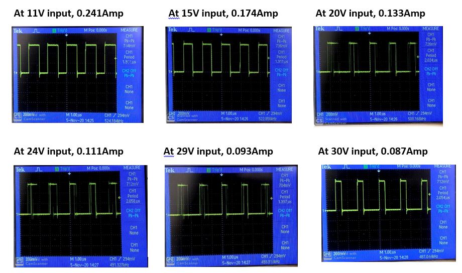
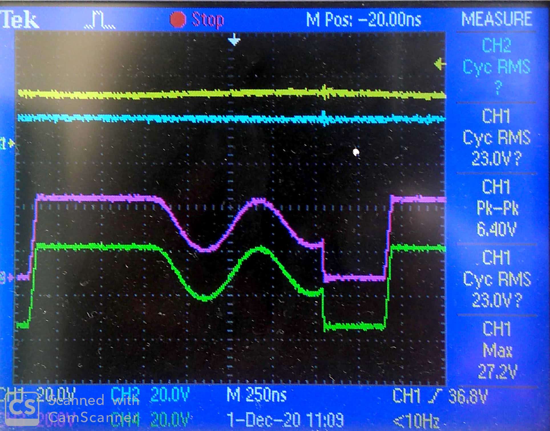
When the input supply voltage is in between 18-30V (0.190-0.160Amp), the SEPIC converter starts making audible noise.

When the input supply voltage is in between 10-18V(0.300-0.189Amp) , there is no such problem of audible noise.

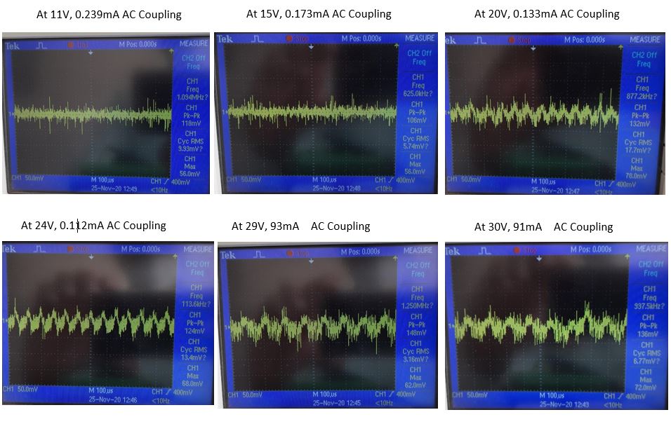
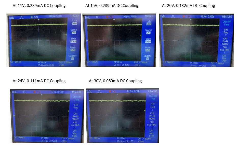
When the input supply voltage is in between 10-30V(0.117-0.093Amp) , there is no such problem of audible noise.

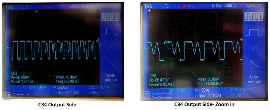
Below is the design of converter. Please let me know if there is any solution to eliminate noise form  SEPIC converter.

  • Hi Yagita,

    Thank you for designing with the LM3481.  It is not very clear whether or not your L4 is connected to the input line. There is missing a junction do. Could you double check, and make sure the schematic is up to date?

    Could you also monitor the voltage of both sides of C34 to GND, when the circuit start producing audible noise?  Please show both zoomed in and zoomed out scope pictures so we can see the overview and also the detailed signal waveforms. 

    Thanks,

    Youhao Xi, Applications Engineering

  • Hi Youhao,

    Thank you for your comments.

    Yes you are right, the design was not complete. The converter has 10-36VDC input. Below is the complete snap of it. 

    I had captured signal waveforms at 24V (0.133Amp) at both the sides of C34 to GND. Below are the zoom in and zoom out pictures of it. Please have a look  and let me know your thoughts on this.

    Thanks,

    Yogita

  • Hi Yogita,

    Thanks for sharing the images. Can you explain what is happening in the C34 Input and Output side photos when the switch node changes shape? Are you doing a load transient there?

    Thanks,

    Richard

  • Hi Richard,

    Thanks for your comments. 

    I am not performing any load transient, the load is stable all the time.

    I had observed gate pulse on DSO, and the signal shows jitter in duty cycle in the range of 20-29V(0.133-0.086Amp) input supply. Please have a look on below snaps taken at different input voltages. The SEPIC converter operates at 10-36V input supply voltage, 12Volt output.

    I am looking forward for your response.

    Thanks,

    Yogita

  • Hi Yogita,

    Thank you for providing the waveforms in addition to the ones provided above. From this, it looks like there may be an issue with the loop stability of the SEPIC converter. One giveaway of that is in your second post on the C34 input side photo. It looks like the part is switching normally, and then the switch node showcases a little glitch before showcasing the sinusoidal behavior.

    Can you take a scope shot of the COMP pin during these conditions, and see if the COMP pin is oscillating? 

    Thanks,

    Richard

  • Hi Richard,

    Sorry for the delay in getting back to you. Please find below snaps from DSO at COMP pin,

    I am looking forward for your response.

    Thanks,

    Yogita

  • Hello Yogita,

    The COMP seems to oscillate with a frequency around 10kHz which might cause audible noise.

    Please send measurements of your output voltage, input voltage, and both sides of the coupling capacitor if possible in one scope plot.

    Did you follow the calculation of the compensation in this app note? 

    https://www.ti.com/lit/an/snva405a/snva405a.pdf

    If yes, please let's make the compensation very slow to stabilize the converter and then check what we need to do to fulfill the system requirements needed on the compensation.

  • Hi Brigitte,

    Thank you for your response. Please find below image which shows waveform for input voltage, output voltage, input side of coupling capacitor(C34) and output side of coupling capacitor. 

    • Yellow : Input Voltage measure across C32 and GND i.e. 24V
    • Cyan   : Output Voltage measure across C35 and GND i.e. 12V
    • Pink    : Waveform across Input side of coupling capacitor C34 and GND
    • Green : Waveform across Output side of coupling capacitor C34 and GND

    I am looking forward for your response.

    Thanks,

    Yogita

  • Hi Yogita,

    It looks like the loop is not stable. Could you measure the loop Bode Plots? 

    Thanks

    Youhao

  • Hi Yogita,

    Long time no hearing from you. I think you have solved the issue. If not, welcome to contact us.

    Best Regards,

    Yichen