Other Parts Discussed in Thread: TPS65185
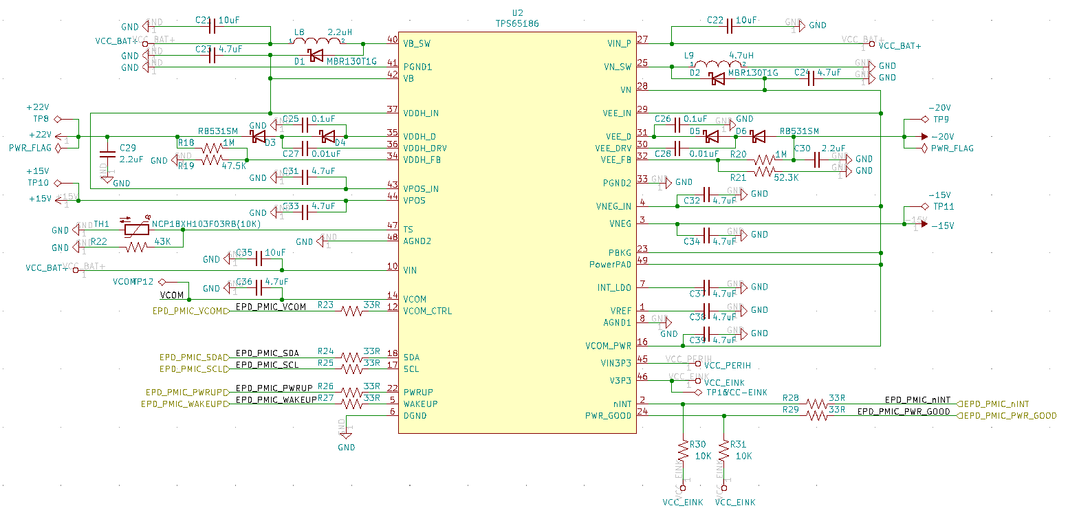
Hello, I have made a board that uses TPS65186. I can read & write the register via i2c protocol, and I can activate it by ENABLE register(I tried PWRUP pin also).
but all power rail not regulated except 3v3(enable register becomes 0x20). and VN_UV interrupt flag is asserted
I have been checked VN & VN_SW. VN_SW generates 1MHz PWM for 100ms. VN generator -4V (not -16V) for 100ms. after that it suspended.
What could be cause??
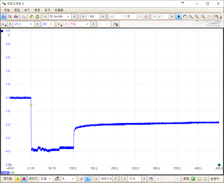
VN voltage
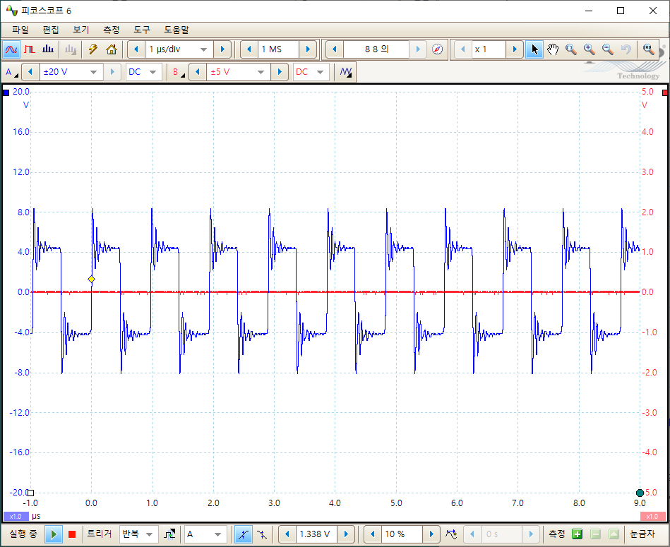
VN_SW PWM Signal
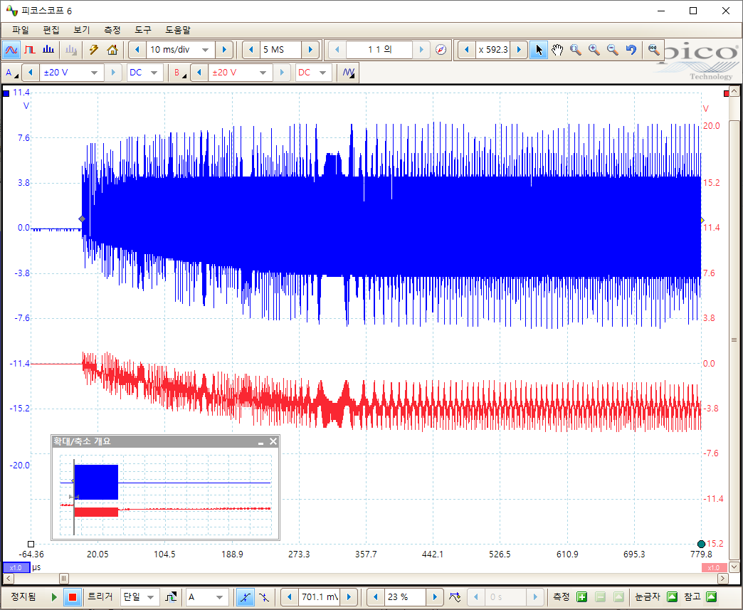
BLUE: VN_SW
RED: VN