This thread has been locked.

If you have a related question, please click the "Ask a related question" button in the top right corner. The newly created question will be automatically linked to this question.

BQ76920: Can the CHARGE and DISCHARGE FET Drivers drive multiple fets?

Part Number: BQ76920
Other Parts Discussed in Thread: UCC27511A-Q1, , UCC27511A, UCC27511, BQ77905

I want to drive 10 N Channel fets on both the Charge and Discharge side.  IRLB3813 that require 57nC of gate charge each.

Can the drivers in the BQ76920 handle this or do I need a more powerful driver?  If so, what do you recommend? UCC27511A-Q1?  Can this driver (UCC27511A) be used on the CHG side, as it it not high impedance when driven low?

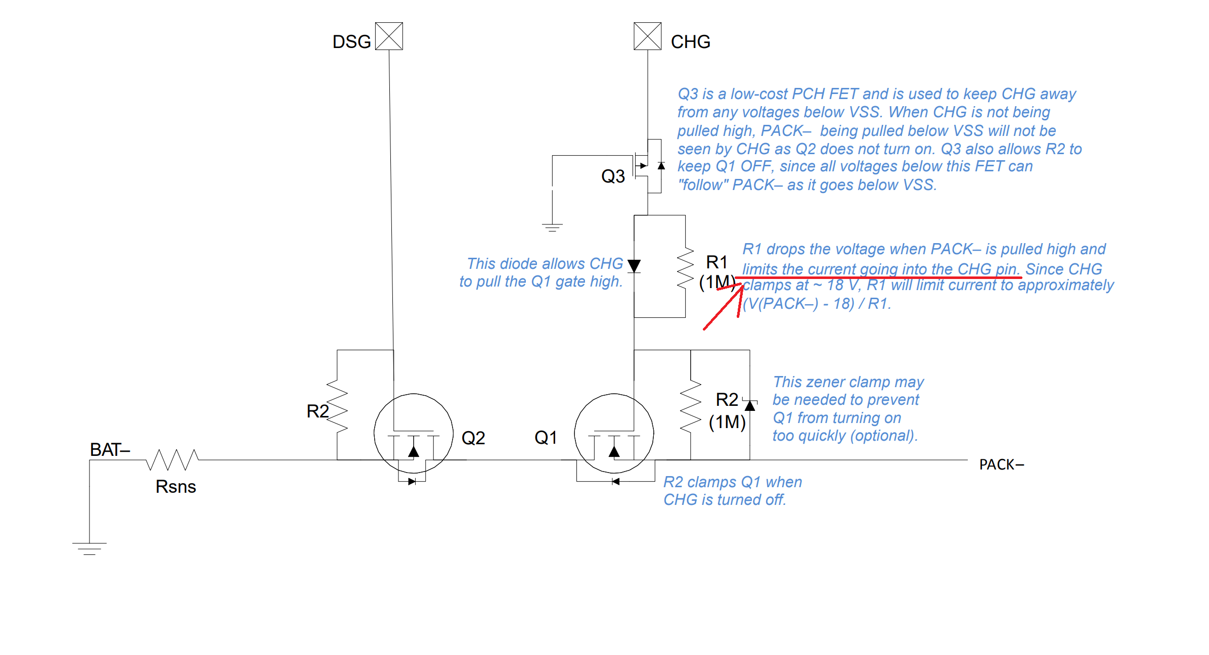
Also, question on why limiting current to charge CHG gate in data sheet?   I am assuming I would want to use a UCC27511A-Q1 low side driver on BOTH DSG and CHG gates.  I would think I would remove diode and R1 and replace with gate driver?  If I have hundreds of amps flowing through CHG and DSG fe's, I woiuld think I switching FETS off as quickly as possible would limit linear region operation.  What am I not considering?

  • Hi FJ,

    Our expert on this device is out today but should be able to respond to your question next week.  From my perspective, I expect it will depend on how fast of a transition you need for the gate signal.  You might look at the FET Drive section of this document:

    https://www.ti.com/lit/an/slua749a/slua749a.pdf

    Thanks,

    Terry

  • I added another question to my post, can you please have an expert take a look at it?

  • Hi FJ,

    10 FETs is a lot and if you have 100's of amps you do want a well controlled turn off and will likely want a stronger driver. The internal driver for the BQ76920 is intended for simple implementations on modest packs. How you do your driver will likely depend on your system requirement.  I'm not an expert on the  UCC27511A-Q1 but it seems a very capable part..  

    In addition to the FET driver section Terry noted in the application note above, keep in mind the range of the PACK- during various system conditions.  The application note https://www.ti.com/lit/pdf/slua773 shows some examples of switching with a device having similar cell count and driver structure to the BQ76920, but with stronger drivers and a built in P-ch FET.  Consider some system conditions:

    • With both FETs on PACK- is about the same voltage as BAT-. Current flows as needed.
    • When the DSG turns off a load will pull up PACK- to PACK+.  See figure 4 of the slua773 apnote.  The large R1 and the parallel diode above limit current into the driver during this condition, BQ76920 has an internal clamp for this condition but with limited current causing the low drive low current.  Note that the UCC27511 does not allow voltage much above VCC.  You may need a provision for that in your design, or an isolated driver for the charge FETs.
    • During SCD the discharge turn off should be fast to limit the high power to a short time, but fast turn off can excite inductance in the cells leading to a high voltage spike on PACK+ and PACK-, as an example see the rise in figure 3 of slua773. You will want to keep that manageable with controlled switching speed or clamp and/or filtering.
    • During charge inhibit on a low voltage battery the PACK- will be below BAT-.  See figure 5 of slua773.   If the charge driver voltage can't go below BAT- the charge FET might come on again.  With a 20V battery and 120% overdrive of 24V many FETs will be conducting.  Your system may be different.  For turn off speed of the charge FETs where current is high, if a technique with a PNP or P-ch FET like section 3 of slua773 does not help you may need a floating driver or float the UCC27511 type driver on PACK- with level shifted input.

    Hope this is helpful. Again the gate drivers have their own set of experts, if you have a question on a driver posting with a driver part number will get you the right people.

  • 1) With either the BQ76920 or the BQ77905 does it list the driver current capability on the data sheets?  I can't seem to find that.  the UCC27511 list as 4A Peak.

    2) The CHG driver goes to high impedance when off, thus relying on the 1M pull down resistor from the CHG fet Gate to Source to turn fet off, correct?  I assume, if correct, that because the charging currents are far less (at least in my case), that a slower turn off time is acceptable?  Do you agree with this?

  • Hi FJ,

    1. The UCC27511 is a general purpose FET driver which is often used for switching supplies where speed is important and ratings are in A indicating a resistance in ohms.  The BQ76920 and BQ77905 list pull down resistances and rise time with the test condition load. For the BQ76920 turn on resistance is approximately 5k. Turn off resistance for battery parts is 10's of ohms to k ohms.  These parts are used specifically for battery switching and is more of a load switch function.  Switching times are often in the 10's of us to avoid the large Ldi/dt response from the cells. Unfortunately the delay from the nominal gate on voltage to the turn off point with R-C of the drive resistance and gate capacitance exponential adds a significant delay to the response time.  

    2. Right.  Initially when CHG is switched low RCHG_OFF (1M) and the external (1M) resistor in parallel with the diode help Rgs pull the gate down, but once the FET starts to turn off with PACK- dropping it is only Rgs which turns off the FET. In smaller packs this is often ok and the designer may adjust the resistor values some.  When the charge currents are high a designer must put more attention and often more circuitry into the turn off of the charge FETs.