This thread has been locked.

If you have a related question, please click the "Ask a related question" button in the top right corner. The newly created question will be automatically linked to this question.

LM5146-Q1: Buck Converter

Part Number: LM5146-Q1
Other Parts Discussed in Thread: CSD19537Q3, LM5145, CSD19531Q5A, CSD19502Q5B

Hi Ti,

I am using LM5146-Q1 for 225W converter i.e VIN 40-60V and Out 15V and 15Aamp.

I have used high and low side mosfet in parallel.

need suggesting what will be the gate resistance ?

Do i need to use separate resistor to each MOSFET or 1 resistor is enough for parallel MOSFET? what is the resistor value need to be consider?

By the thermal camera i could see the gate trace for lower MOSFET feel temperature rise do i need to increase the resistance or any pull down resister need to use.

Another issue i have, at no load the low side 1 MOSFET have temperature rise more than other  , while i kept the some load both mosfet temperature came equal or start cool.


1 time the LM5146-q1 get hot and it went bed.

Please suggest.

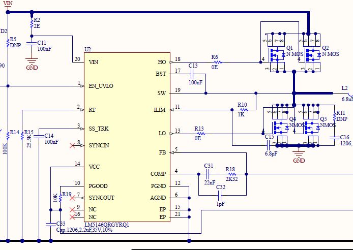
  the upper mosfet is CSD19537Q3

and low: FDWS86068-F085

  • Hi Dinesh,

    See the LM5145 EVM (5V/20A/225kHz) design as it is similar to this applicable. Please use 5 x 6 mm MOSFET packages for this application as it provides much better thermal performance.

    Also, please complete and send the LM5146Q1 quickstart calculator so we can review power stage component power losses. The file is available in the product folder. In terms of gate resistance, a 1 or 2.2Ohm in series with the boot cap is sufficient (nothing on the low-side FET).

    Regards,

    Tim

  • Hi Tim,

    I have attached as pdf,

    waiting for the comment on my previous 3 questions:

    1. :>   Do i need to use separate resistor to each MOSFET or 1 resistor is enough for parallel MOSFET? what is the resistor value need to be consider?

    2.: >   By the thermal camera i could see the gate trace for lower MOSFET feel temperature rise do i need to increase the resistance or any pull down resister need to use.

    3:> Another issue i have, at no load the low side 1 MOSFET have temperature rise more than other  , while i kept the some load both mosfet temperature came equal or start cool.


    1 time the LM5146-q1 get hot and it went bed.

    LM5146-Q1 Quickstart Tool r2 - 48Vin 15Vout 15A 400kHz.pdf

  • Hi Dinesh,

    You can use separate gate resistors for the high-side FETs (if needed). No resistors are required for the low-side FETs. In my opinion, one correctly chosen high-side FET in 5 x 6 mm package is sufficient given the low duty cycle.

    Looking at your quickstart file, the loop is very much unstable. Please use the recommended compensation components. Also, update the MOSFET parameters so you can review the losses.

    The gate drive traces (HO and SW, LO) should be > 20 mils wide and should not have any temperature rise.

    Regards,

    Tim 

  • By the way, a 12mOhm inductor dissipates too much power at 15A. Consider using a 4.7uH and lower DCR. For the output cap, make sure any ceramic devices are correctly derated for the output voltage -- enter the correct cap value and ESR in the quickstart to accurately determine the compensation components.

  • Hello Tim,

    The compensation resistor and capacitor has been taken from WEBENCH and i am not sure which one have to follow excel sheet or webench.

    why at no load the low side 1 MOSFET have temperature rise, while i kept the some load both mosfet temperature came equal or start cool.

  • Hi Dinesh,

    Please forward the switching waveforms at no load for review. I suspect it is capacitive loss related to gate drive and hard switching at high-side turn off.

    In terms of compensation, please review the recommended compensation values from the quickstart and the associated bode plot to ensure stability.

    Regards,

    Tim

  • Hello Tim,

    i have take the resistor and capacitor value for companion  from Webench and it is not match to excel sheet .

     Do you suggest not to follow webnch ,used only excel sheet ?

    What about sync in pin , i did not connect to GND.

    i will send wave form soon.

    Thanks,

    Dinesh Gread

  • Dinesh,

    Use the quickstart as it matches the datasheet equations. Just ensure that any ceramic output cap is correctly derated for voltage.

    The is an internal 20k pulldown on SYNCIN, so the pin is effectively low if left open.

    Regards,

    Tim

  • Hi Tim,

    i am redesigning my converter and as per suggestion of webench i am using single Mosfet for Top and Single Mosfet for Lower The part number for Top : CSD19531Q5A And Lower is FDWS86068-F085

    Are you suggested same for the converter.

    or i need to use 2 Mos for uper or 2 for lower.

    i am attaching the excel file please share your view .MOSFET name is not able to edit rest of all data match to update given part number.

    Thankyou.LM5146-Q1 Quickstart Tool r2 - 48Vin 15Vout 15A 310kHz.pdf

  • Hi Dinesh,

    Here are some comments on the quickstart:

    1. Current limit should be ~150% of rated full load current.
    2. Output cap of 880uF is quite high for a 15V output. Use 3-4pcs of 22uF/25V ceramic should be fine.
    3. Note the ESR provided is very high - the ceramics will reduce this dramatically (a few mOhms).
    4. Input caps near the FETs should be ceramic, e.g. 3-4 pcs of 4.7uF/100V.
    5. Use 80V FETs for best efficiency given that Vin-max is 80V (see the LM5145 5V/20A EVM). This would allow one FET each for the HS and LS positions. However, this also depends on max ambient temp spec and availability of airflow.

    Regards,

    Tim 

  • Hi Ti,

    Thanks for reply

    1. Current limit should be ~150% of rated full load current.  ::::::::>                                                                                                                                                   i want to limit the current near 15 Amp only so no body shoud use more than that.
    2. Output cap of 880uF is quite high for a 15V output. Use 3-4pcs of 22uF/25V ceramic should be fine.::::>                                                                     22ufx5 cap is enough ? 
    3. Note the ESR provided is very high - the ceramics will reduce this dramatically (a few mOhms).::::> Agree
    4. Input caps near the FETs should be ceramic, e.g. 3-4 pcs of 4.7uF/100V. ::::::::::>                                                                                                              It is added in schematic
    5. Use 80V FETs for best efficiency given that Vin-max is 80V (see the LM5145 5V/20A EVM). This would allow one FET each for the HS and LS positions. However, this also depends on max ambient temp spec and availability of airflow.   :::::::::::>                                                                             i have checked that EVM but in that NVMFS6B25NLT1G & NVMFS6B14NL both RDSon is to high what i have used .So request you to please comment on the MOSFET  top CSD19531Q5A And Lower is FDWS86068-F085.

  • Hi Dinesh,

    I inserted some answers below.

    Regards,

    Tim

    Dinesh Gread2 said:

    Hi Ti,

    Thanks for reply

    1. Current limit should be ~150% of rated full load current.  ::::::::>                                                                                                                                                   i want to limit the current near 15 Amp only so no body shoud use more than that. [TH] If 15A is the OCP setpoint, then the rated full-load current is typically below that. Note there is some variation in the OCP setpoint, hence the requirement for some margin. Also, note that the inductor current can overshoot during a load transient.
    2. Output cap of 880uF is quite high for a 15V output. Use 3-4pcs of 22uF/25V ceramic should be fine.::::>                                                                     22ufx5 cap is enough ? [TH] Yes, sounds fine..
    3. Note the ESR provided is very high - the ceramics will reduce this dramatically (a few mOhms).::::> Agree
    4. Input caps near the FETs should be ceramic, e.g. 3-4 pcs of 4.7uF/100V. ::::::::::>                                                                                                              It is added in schematic
    5. Use 80V FETs for best efficiency given that Vin-max is 80V (see the LM5145 5V/20A EVM). This would allow one FET each for the HS and LS positions. However, this also depends on max ambient temp spec and availability of airflow.   :::::::::::>                                                                             i have checked that EVM but in that NVMFS6B25NLT1G & NVMFS6B14NL both RDSon is to high what i have used .So request you to please comment on the MOSFET  top CSD19531Q5A And Lower is FDWS86068-F085. [TH] In general, 80V FETs are more efficient than 100V devices - see what we used on the LM5145 5V/20A EVM. However, the 100V FETs you have seem okay, just keep the Fsw below 250kHz to reduce switching losses.

    Hi Dinesh,

    Here are some comments:

  • Hello Tim,

    In the EVM you suggested the upper MOSFET has been used from Infineon BSC117N08NS5 the Rdson is high approx 12mE So i am going to use in my design CSD19502Q5B from Ti rds on is approx 3.5mE

    Lower Mosfet : BSC037N08NS5 is fine for me as its Rds on is approx 3.4mE

    Thanks,

    Dinesh Gread

  • Hi Tim ,

    I have send the query to MOS manufacturer they will suggest me ACE qualified part I will update you with new part number.

    i have another query with current limiter circuit i have made a circuit to provide a limitation on output current .but i feel the voltage is passed through the diode in low current also before 0.7V vf. for example i have connect a 3 Amp load and the voltage generate by the op amp & voltage divider is in mV.

    Still that mV value pass the diode now i have FB 0.85 which should be after 14 Amp. Could you please suggest any correction.i am using same feadback path for limiter. Looks like this is disturb the feadback path.

  • Hi Dinesh,

    See app note snva829 for more detail on constant current limitation using an output shunt.

    https://www.ti.com/lit/an/snva829/snva829.pdf

    The LM5146-Q1 also provides current limiting but will enter hiccup and restart if an OCP condition occurs.

    Regards,

    Tim

  • Hi Tim,

    Can i use OCP as a current protector ,as my OCP may vary due to Rds & Temprature and it is acceptable for me as i dont have very strict value , i only require that no body use converter more than 15 Amp and in short circuit protection.

  • Yes, shouldn't be a problem, that's the purpose of the OCP function.

    Regards,

    Tim

  • HI Tim,

    At the low side MOS the voltage spike is high at no load condition once i add some load like 300mA  the spike will reduce.

    The attached waveform i have taken of VDS at low side mos, at 58 Volt the spike is going upto 170V pk. this may harmful for Low side mos as the VDS of MOS is 80 or 100 Volt.

    Could you please let me know the reason & solution to reduce the same.

    Now i have reduced the sw frequency to 215 kHz

  • Take a look at app note snva803 for power stage layout. Looks like you have a lot of parasitic inductance.

  • Hi Tim,

    how to reduce it now , do i need to use some type of snubber or TVS parallel to low side mosfet?

  • Sure, try a 2.2Ohm and 470pF from SW to GND. And add a 10 Ohm boot resistor.